


PCB design for manufacturability is an indispensable part of modern electronics design. With rising cost, miniaturized
designs, and higher speed components, companies have very little room for errors as far as mass production is concerned.
Without a sound design for manufacturability (DFM) strategy, companies are at risk of costly post-production flaws.
Contents
- 1 What is Design For Manufacturability?
- 2 Why It’s Important To Apply DFM In PCB Design?
- 3 PCB Design For Manufacturability Tips
- 4
- 5 1. Sufficient Edge Clearance
- 6 2. Add Fiducial Markers
- 7 3. Precise and Visible Component Designators
- 8 4. Standardized IC Orientation
- 9 5. Single Side Component Placement (If Possible)
- 10 6. Ensure Correct Solder Mask Clearance
- 11 7. Avoid Via In Pads
- 12 8. Ensure Sufficient Annular Ring Size
- 13 9. Prevent Acid Traps
- 14 10. Check For Copper Slivers
- 15 Summary
What is Design For Manufacturability?
Design for manufacturability, or DFM, refers to optimization strategies that ensure electronic products are consistently
functional, reliable, and durable upon fabrication and assembly. DFM is prevalent in modern product development as
manufacturers are hard-pressed to minimize cost and wastage during production.
Why It’s Important To Apply DFM In PCB Design?
It’s a fact that the quality of PCB fabrication and assembly relies on humans and machines. Both are subjected to flaws
as PCB fabricators and assemblers operate optimally when certain conditions are met.
DFM serves as a bridge between hardware designers and PCB suppliers. It ensures that both parties are agreeable on
manufacturing parameters such as drill size tolerance, trace spacing, and tooling setup.
With DFM, PCB assemblers do not need to second-guess how and where components are placed. It also eliminates issues like
barely-visible short circuits due to close proximity pads or the absence of solder masks.
Failure to make DFM a part of PCB design strategy leads to costly recalls, reworks, and unhappy customers. DFM minimizes
incidences of rejects and technical issues that materialize after deployment. By rigorously optimizing the PCB for
manufacturing, companies will see remarkable post-production financial savings.
PCB Design For Manufacturability Tips
There’s a great difference between producing a handful of prototypes and thousands of reliable, fully functional PCBs.
Therefore, it’s crucial to ensure that your design complies with this PCB DFM checklist before producing in volume.
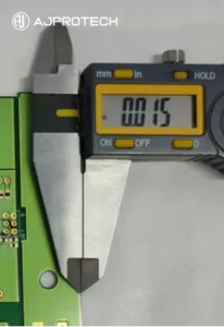
1. Sufficient Edge Clearance
Understandably, you’ll want to minimize the PCB dimension for a more compact design. However, populating
components and copper traces at the edge of the PCB will spell trouble. It’s essential to maintain a sufficient
edge clearance on the PCB for both fabrication and assembly. During PCBA, traces placed too close to the edge
may not be sufficiently protected by the insulative coating. This will cause the traces to suffer from potential
short circuits. Ideally, you’ll want a 15 mil spacing between copper trace and the PCB edge. Also,
pick-and-place machines require a narrow space to grip onto the PCB. If the PCB is populated to the edge,
automated component placement may not be possible. You can fix this DFM issue by adding tooling strips on both
sides of the PCB.
2. Add Fiducial Markers
Fiducial markers are tiny copper dots enabling accurate alignment on the pick and place machine. At least 3
fiducial markers need to be placed on the edge of the PCB or tooling strips for precise alignment and placement.
These are called global fiducials.
If your PCB is considerably large and there are small-pitched (< 1.0mm) SMT ICs, you’ll need to add local
fiducial markers diagonally along the edge of the component’s footprint.
3. Precise and Visible Component Designators
Do not underestimate the importance of component designators regardless of whether the PCB is manually or
machine assembled. Component designators aid the assembly process and are equally important for rework or
repair.
Ensure that component designators are of the right dimension. They should also be placed systematically and near
the respective components. You don’t want assemblers having trouble matching components to the designators or
technicians fixing the wrong parts.
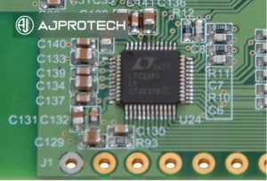
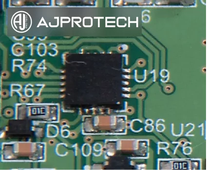
4. Standardized IC Orientation
All semiconductor ICs have an orientation mark. It could be a printed dot on pin one or a notch on the package.
Either way, it’s essential to keep all ICs aligned in the same direction. Doing so prevents confusion when
assembling the ICs on the PCB and also improves efficiency.
{SNIPPET=373}
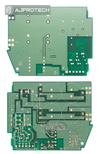
5. Single Side Component Placement (If Possible)
Component placement can determine the complexity of the assembly process and hence, production cost. Sometimes,
it’s tempting to reduce board size by placing components on both sides of the PCB.
However, doing so means doubling the component placement process, including producing two solder paste stencils.
By populating all the components on the same surface, you’ll enjoy a noticeable reduction in the assembly cost
per unit.
6. Ensure Correct Solder Mask Clearance
Solder mask is a thin layer of solder-resist polymer added to the PCB during fabrication. It prevents solder from
forming unwanted joints or attaching to copper traces. Component pads must be free from solder masks for proper
soldering to take place.
Therefore, it is important to ensure that solder mask clearance is set to the correct parameters. The solder mask
should never be smaller than the pad, or it would affect its solderability. Ideally, you’ll want to compensate for
process misalignment with solder mask expansion of at least 4 mils.
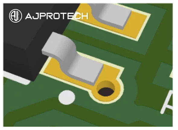
7. Avoid Via In Pads
This is another classic DFM issue that happens when designers attempt to minimize PCB size. It’s common for SMT
ICs to be fanned out with vias. However, shifting the via to an overlapping position with the pad brews trouble.
It leads to a weakened solder joint, which affects the mechanical and electrical stability of the component.
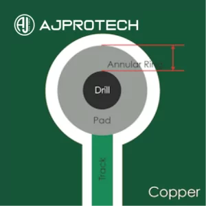
8. Ensure Sufficient Annular Ring Size
Whether it’s a through-hole pad or via, they go through the same fabrication process. Both require a minimum
annular ring size to prevent drilling complications. For example, the drilling process may not be 100% accurate,
and an undersized annular ring may result in the hole overlapping with an adjacent conductive trace.
Preferably, you’ll want to have an annular ring size of at least 6 mil.
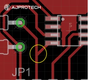
9. Prevent Acid Traps
The negative effect of acid traps only materializes after a while. An acid trap is caused by awkward copper
geometry that results in the entrapped etching solution. This is often the case when you have narrow angled
(<90°) copper traces, which prevents the etching solution from being properly washed off.
While some manufacturers have adopted alkaline etching, it’s still a good DFM practice for your design to ensure
traces are bent at 45°.

10. Check For Copper Slivers
Copper slivers are tiny strips of copper extending from a copper pour and forming a connection with a via or
pad. They are commonly seen in ground planes where thin strips of copper join ground pads to a large polygon
pour.
You’ll want to run a check for copper slivers and increase their size as the etching process may remove
overly-thin copper from the PCB. This results in disconnectivity between the pads and the larger copper plane.
Summary
A good DFM strategy is needed to mitigate modern challenges in electronics product development. We’ve shown you the key
DFM checks that will lead to improved yield and profitability.
If you’re unsure if your design is optimized for DFM, talk to our team, and we’ll be more than happy to help.
AJProTech is the premier product engineering consultancy for smart, connected products. We help companies build
innovative, connected hardware faster.