Hardware Product Development

Hardware development from idea to production
At AJProTech, we blend innovation with execution to create industry-leading products. With over 55 successful projects, our Proven Process ensures efficient and cost-effective product development.
Our Proven Process includes:
- In-depth Research
- Rapid Prototyping
- Detailed Industrial Design
- Software and Firmware Development
- Advanced PCB Design
For those familiar with product development, the critical workflow steps are:

HARDWARE DEVELOPMENT: RESEARCH IS ESSENTIAL
The hardware product development is a complex journey that involves several critical stages. It begins with comprehensive research to understand market needs and technological possibilities. This is followed by the feasibility stage, where ideas are evaluated for their practicality and potential success. The subsequent design phase creates detailed prototypes to refine the product’s features and aesthetics. Rigorous testing ensures reliability and compliance, addressing any potential issues. Finally, the process culminates in mass production, where manufacturing is scaled up while ensuring the product meets high quality standards. Each stage is essential in transforming an idea into a market-ready product.
The journey from concept to a market-ready product spans 1 to 2 years, though it can take longer. Adhering to this structured process is essential for success. Here is a closer look at our process:
Our diligent research and development processes are designed to transform innovative ideas into reality, providing a clear path from concept to completion.
Research:
Market analysis and user need assessment to identify the problem and potential solutions.
Prototyping:
Creation of functional prototypes to demonstrate proof of concept and refine product features.
Industrial Design:
Focus on aesthetics and user experience to ensure the product is both functional and visually appealing.
PCBs:
Detailed design and testing of printed circuit boards to ensure reliability and performance.
Software and Firmware:
Development of reliable software solutions and firmware to support the product’s functionality.
Each stage involves rigorous testing and validation to confirm the design’s feasibility and readiness for production. Following our Proven Product Development process—encompassing Research->EP -> EVT->DVT ->PVT—is critical in navigating the complex journey from idea to market-ready product.
By choosing AJProTech, clients benefit from our extensive expertise and innovative approach, ensuring their products exceed industry standards. Let’s bring your vision to reality!
RESEARCH IS ESSENTIAL
User-Focused Ideation
When clients share their product concepts, we immerse ourselves in understanding the problem they aim to solve, the target audience, essential features, and desired pricing. This deep understanding helps us align our approach with the client’s objectives, ensuring we create a product that fulfills their vision.
Extensive Solution Research
We conduct detailed research to pinpoint the core technologies essential for the product’s success. This involves analyzing existing market products, reviewing patents, and identifying key technologies. This critical phase helps us identify potential technical challenges and develop innovative solutions to overcome them.
Detailed Specifications Blueprint
After identifying the necessary technologies, we craft detailed product specifications. These documents cover operating and storage conditions, mechanical and electronic requirements, and pricing considerations. Our carefully prepared specifications serve as a roadmap, ensuring that the development process remains on track and meets client expectations.
Visualizing: sketches
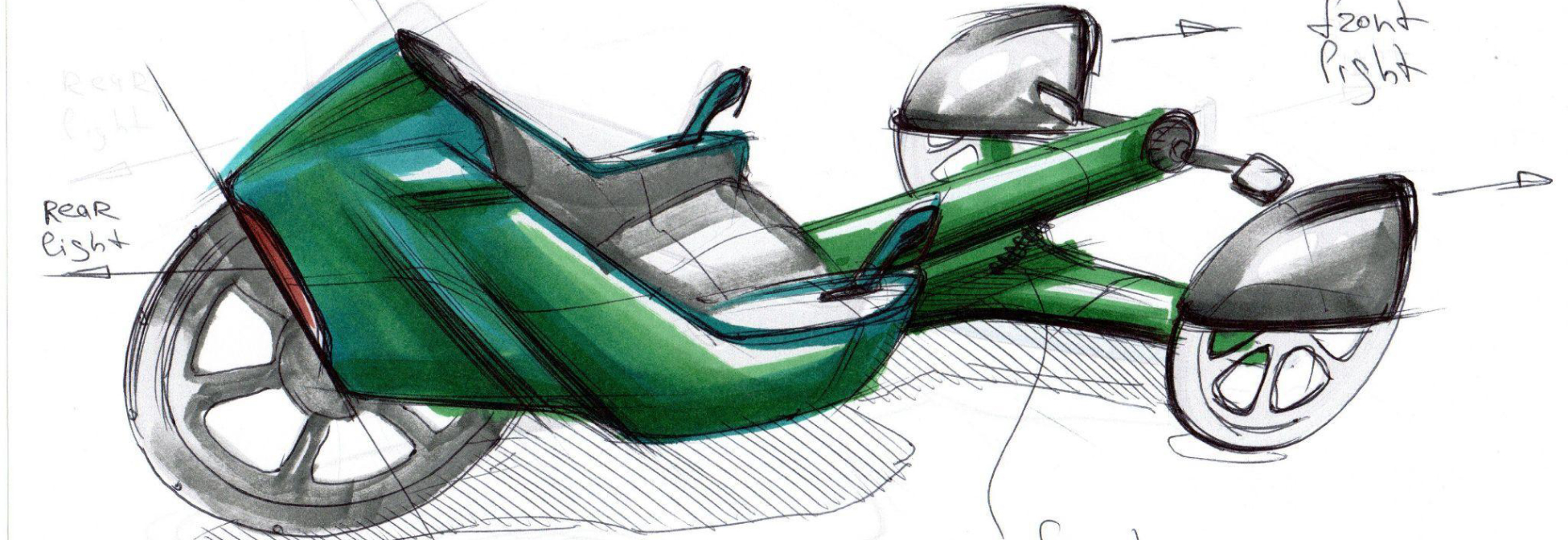
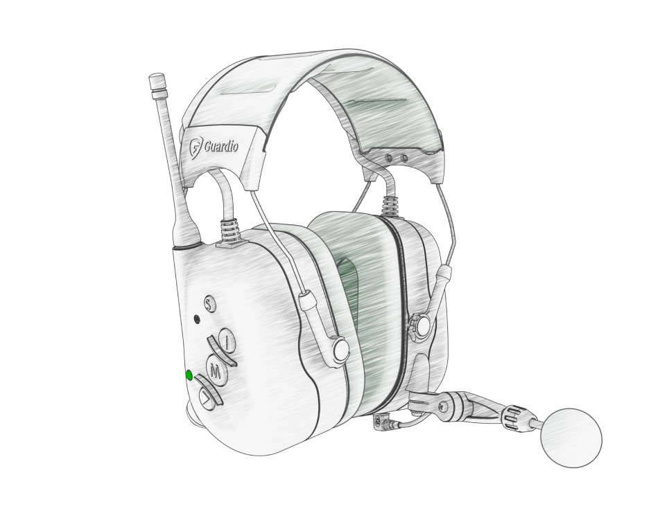
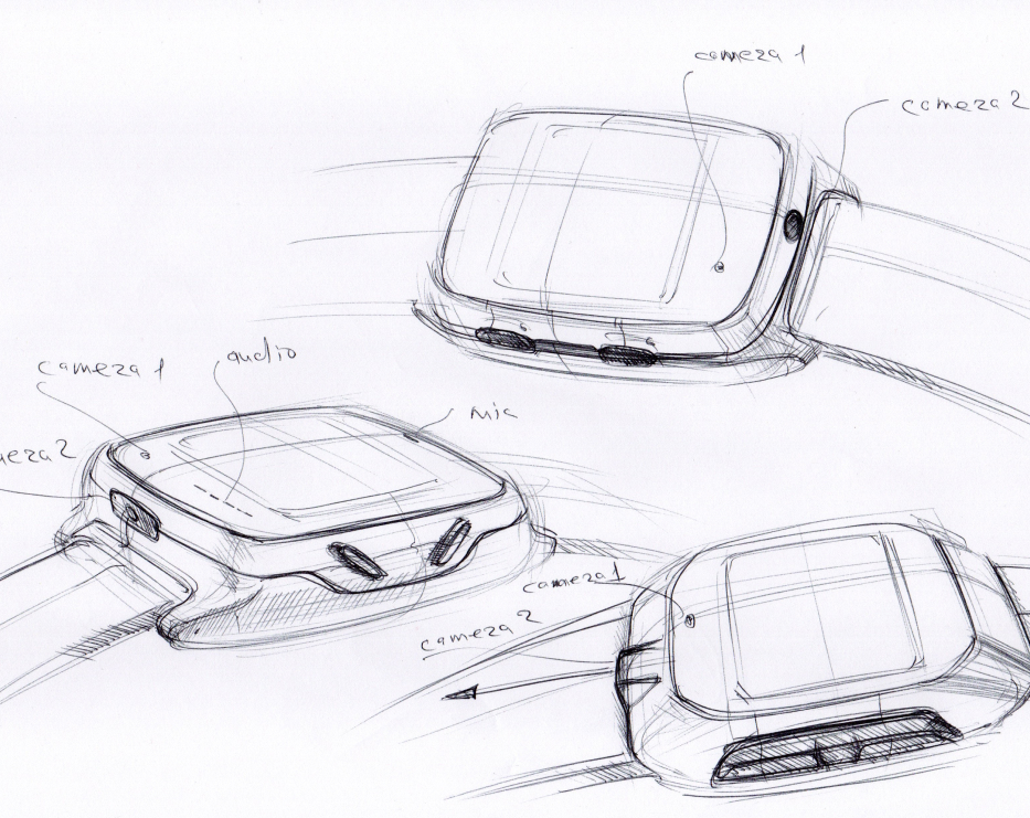
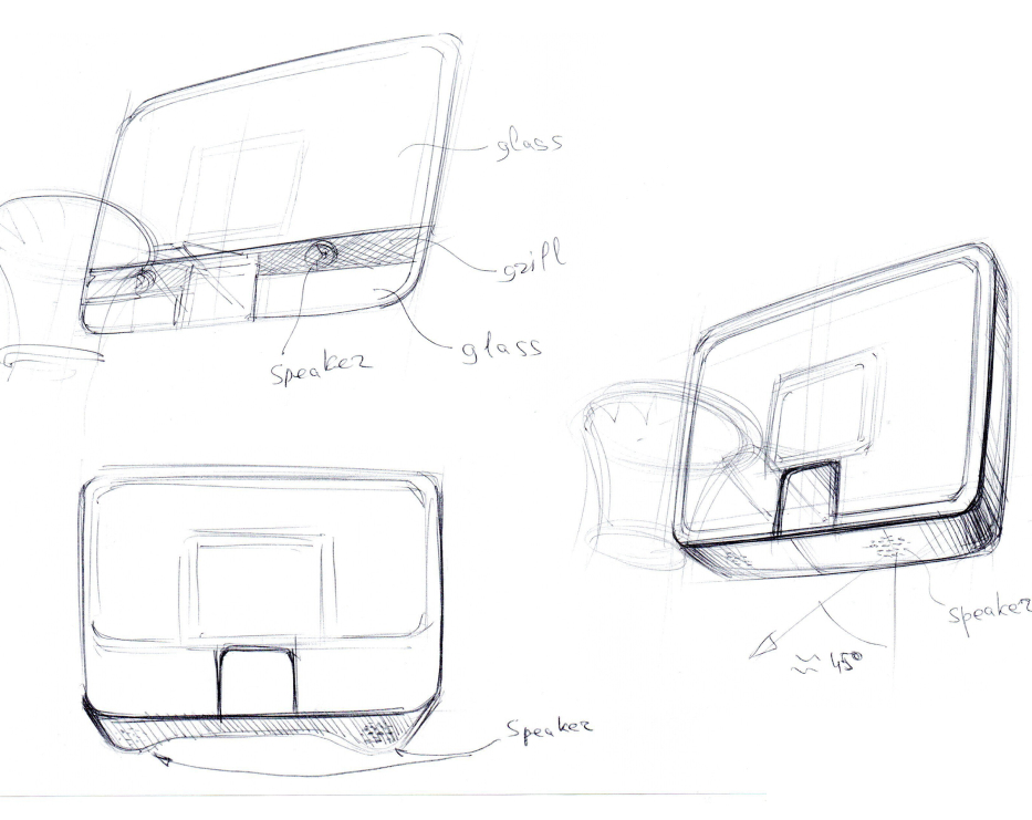
Humans are inherently visual. To truly engage stakeholders and generate excitement, a working prototype isn’t enough; they need to see the envisioned product. That’s why our feasibility study incorporates detailed sketching by our expert industrial designers. These low-fidelity sketches serve as the initial steps in defining the product’s form and function.
By visualizing the device early in the development process, we can make critical adjustments before advancing to prototyping and production. This iterative design phase allows us to explore a variety of shapes, sizes, and materials swiftly. Typically, we create 10 to 15 sketches, selecting a few promising ones for further refinement.
Through this meticulous process, we fine-tune the design, addressing any potential issues that may arise. These sketches not only streamline future design iterations but also anchor the product design trajectory, ensuring alignment with the original vision.
SEEING IS BELIEVING: RENDERS
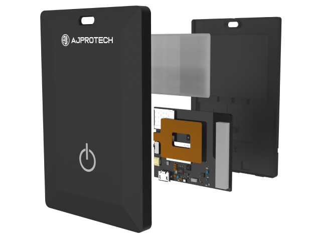
Once we've identified the most promising sketches, our focus shifts to producing high-quality 3D renders. These visualizations offer critical insights and preliminary measurements, empowering our mechanical engineers to make informed decisions throughout the development process. Beyond aiding the engineering team, these renders also serve as powerful tools for marketing and promotional activities.
What can we create together?
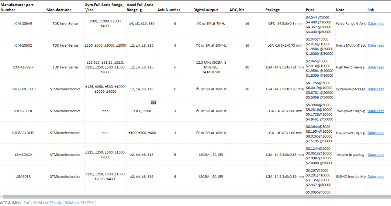
COMPONENTS SELECTION
The component selection phase involves a thorough evaluation of the trade-offs between different components. This is done by intensive research, simulations and tests to validate the performance of each component. The team considers the potential risks and uncertainties associated with each component, including supply chain disruptions, manufacturing issues, and regulatory compliance. By carefully selecting the right components, our product development team can ensure that the final product meets customer expectations, is reliable, safe and can be easily maintained and repaired.
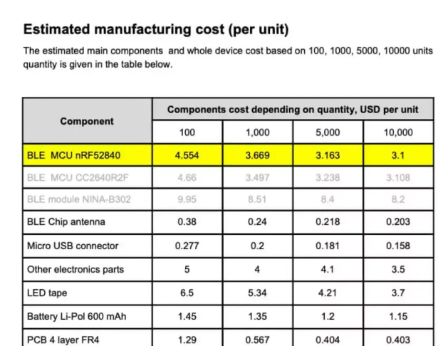
After choosing the components, we recommend creating a Bill of Materials (BOM). This will allow you to accurately calculate the cost of all the individual components required for manufacturing the product. A BOM typically includes a list of all the necessary materials, their quantities, and their respective costs. By creating a BOM, you can ensure that you have a clear understanding of the total cost involved in producing your product, which can help you make informed decisions about pricing and profitability.
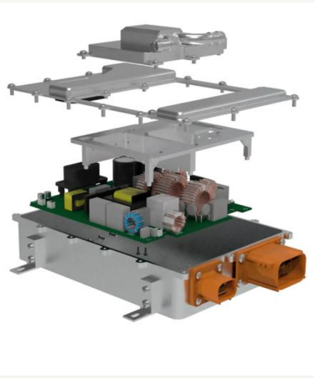
MECHANICAL DESIGN: COMPONENTS PLACEMENT
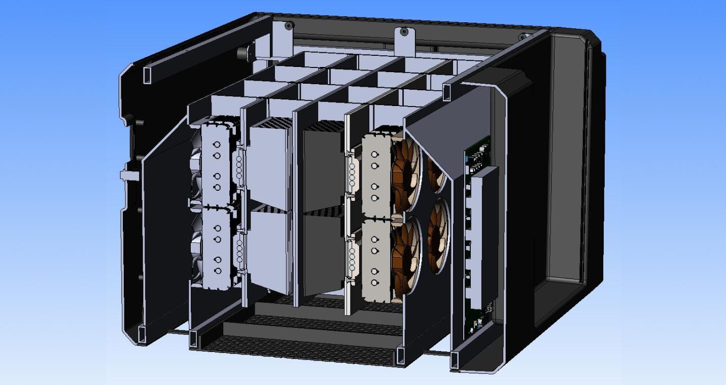
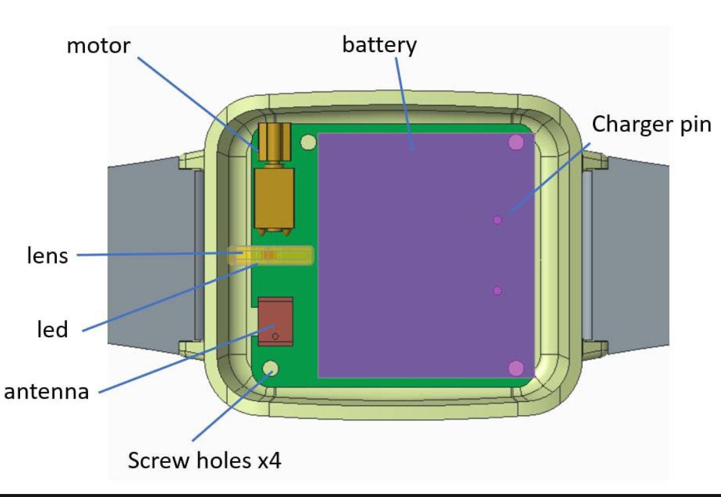
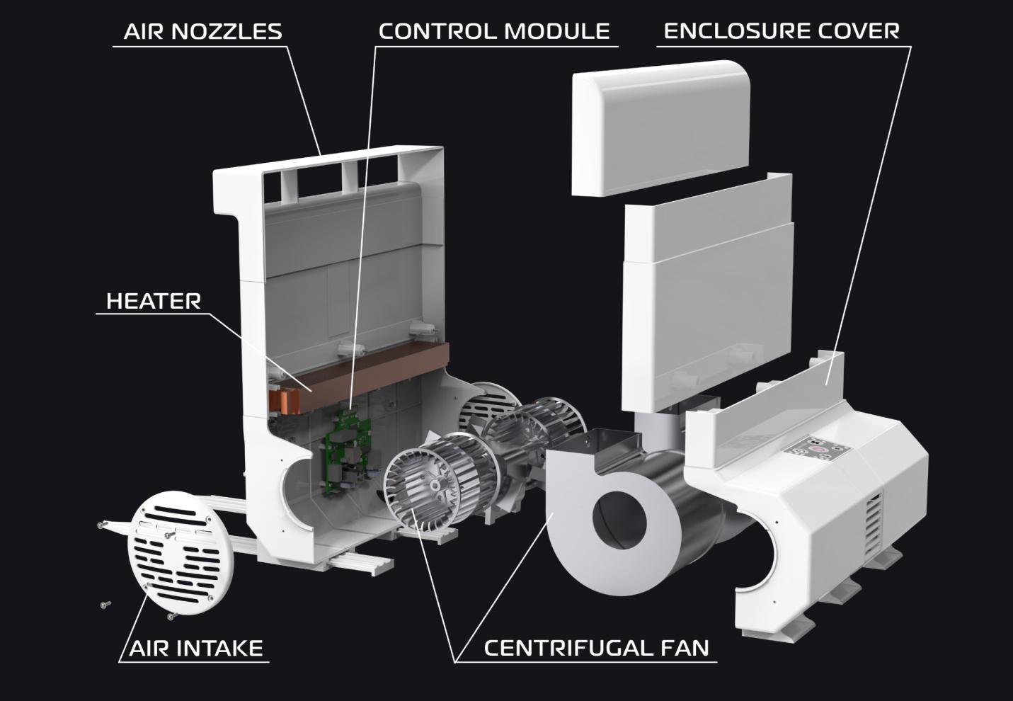
After the design phase is done and approved - it’s time to see how all components are placed together in the enclosure. This process can go in parallel with the next two.
The strategic placement of components plays a crucial role in enhancing both the aesthetics and ergonomics of a device. By meticulously arranging components to achieve a visually pleasing and user-centric layout, our development team ensures a more intuitive and user-friendly experience for the end user.
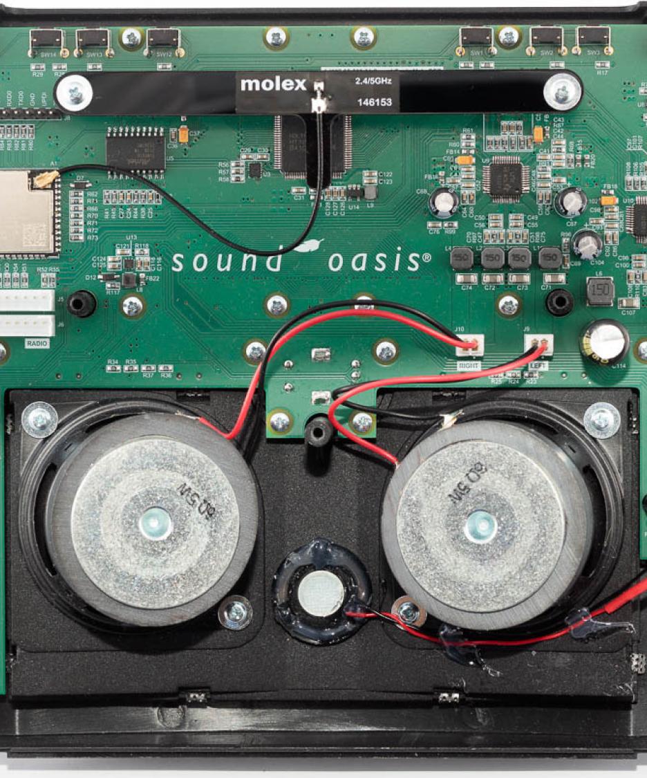
Proper placement of components, such as microprocessors, memory chips, and other essential components, can help ensure that they are properly cooled, ventilated, and protected from physical damage. Сareful consideration of component placement can also help reduce electromagnetic and radio-frequency interference , which can be important in applications where signal integrity is critical.
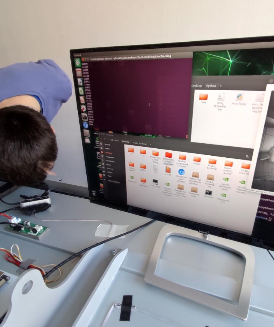
Duct tape PROTOTYPES
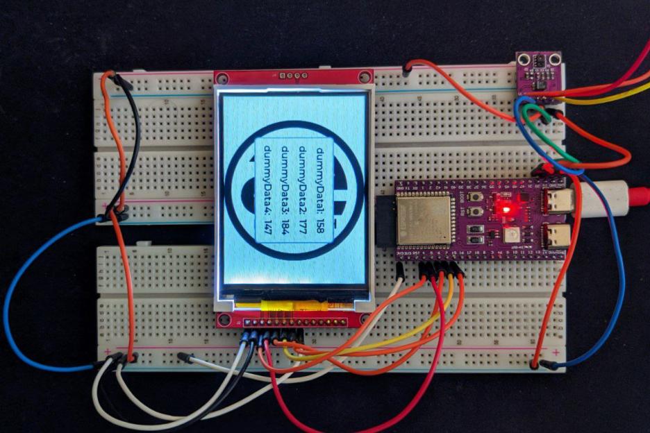
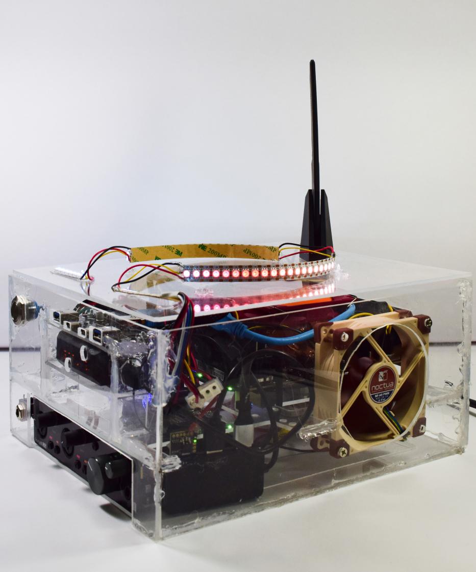
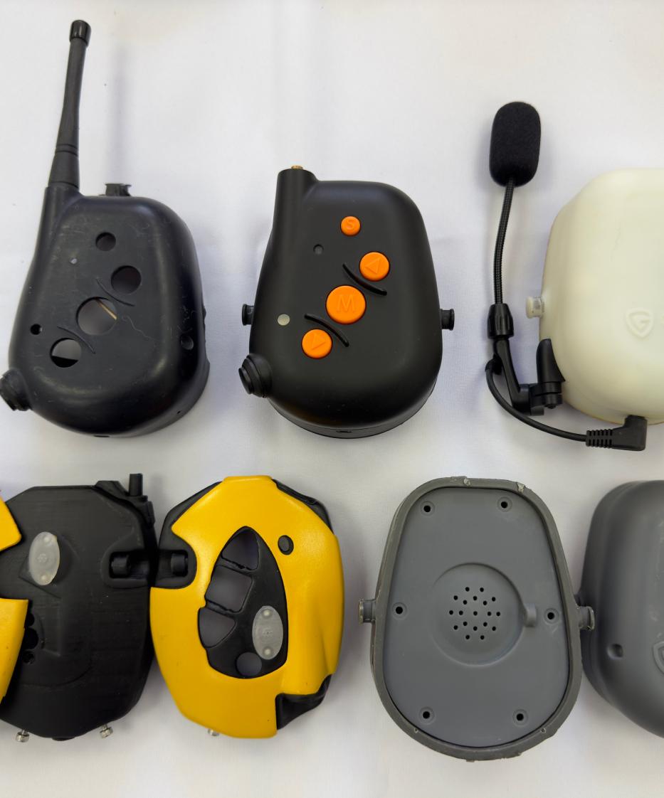
Prototyping in product development, especially in tech and IoT, is crucial for exploring concepts and refining designs. Two primary prototype types are Proof of Concept (PoC) and Work-Like prototypes. PoC prototypes demonstrate the feasibility of an idea or feature, focusing on technical execution, validating key assumptions, and identifying challenges without a fully functional product.
Work-Like prototypes provide a more comprehensive representation of the product, emphasizing functionality and user interactions while also focusing on product quality. Developed after a PoC has confirmed the concept’s feasibility, Work-Like prototypes replicate essential aspects of the final product. They create opportunities for teams to test specific features, gather insights from users, and refine the overall design. By simulating real-world scenarios, these prototypes help ensure that the product not only meets technical specifications but also aligns with user needs and expectations.
Together PoC and Work-Like prototypes contribute to informed decision-making, risk mitigation, and the successful launch of products that are both innovative and market-ready.
ELECTRICAL ENGINEERING:
FUNCTIONAL DIAGRAM AND SCHEMATICS
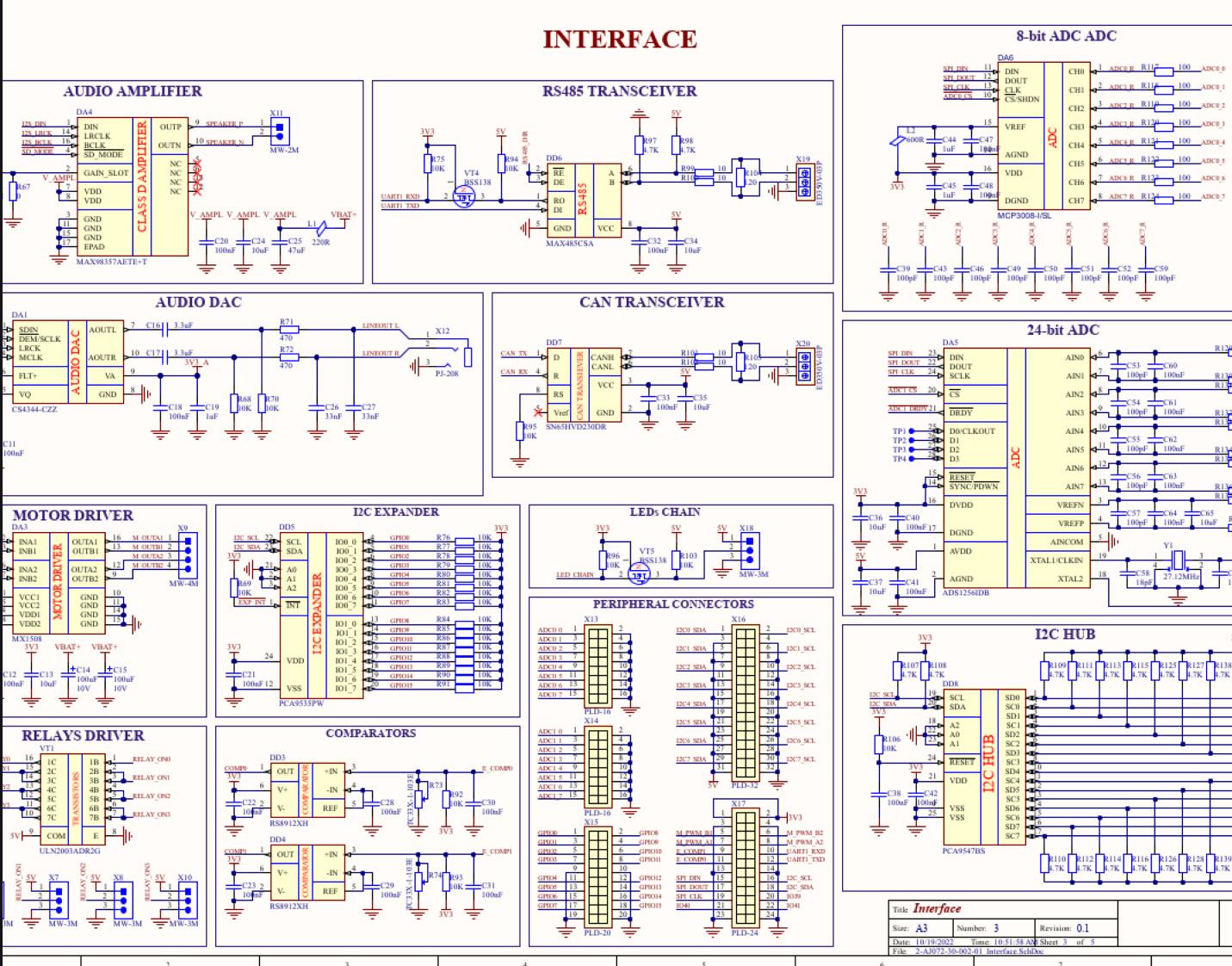
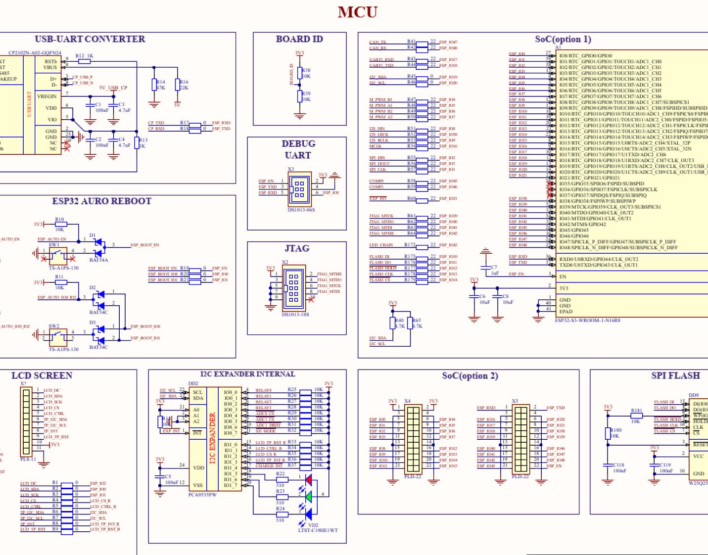
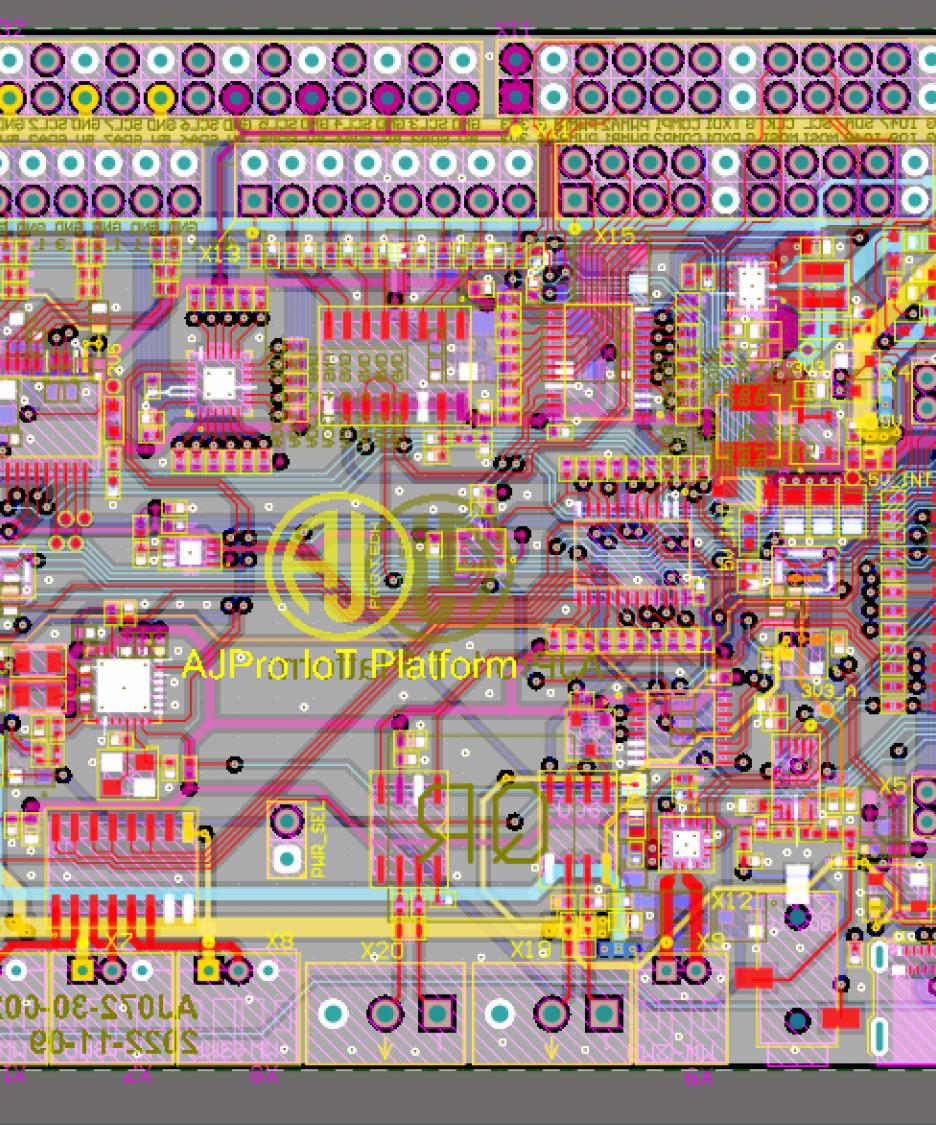
Once all components have been selected, the next step is to determine their optimal placement within the system. Initially, we prepare a functional diagram to identify any potential issues in the design. While this initial diagram is often straightforward, it effectively outlines the interactions and workflows of all critical components.
Following this, we develop a more detailed functional diagram. This process can occur concurrently with the placement of components and the breadboard testing phase.
The detailed diagram serves as an essential resource for hardware engineers, enabling them to analyze and refine the design to ensure it meets all required specifications and is prepared for the subsequent phases of development. Due to confidentiality agreements (NDAs), we will refrain from including numerous images, as they tend to be similar and may compromise sensitive information.
FIRMWARE
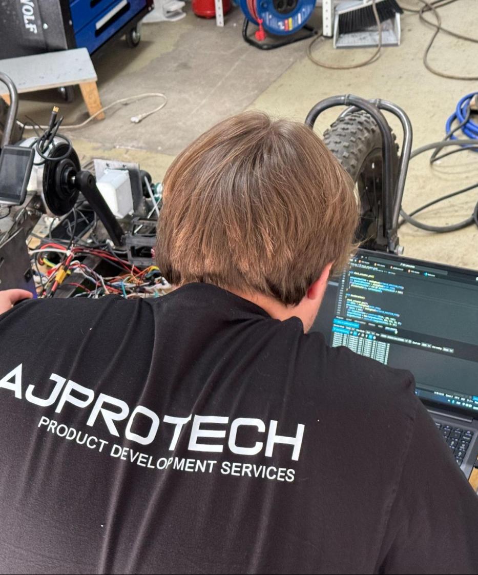
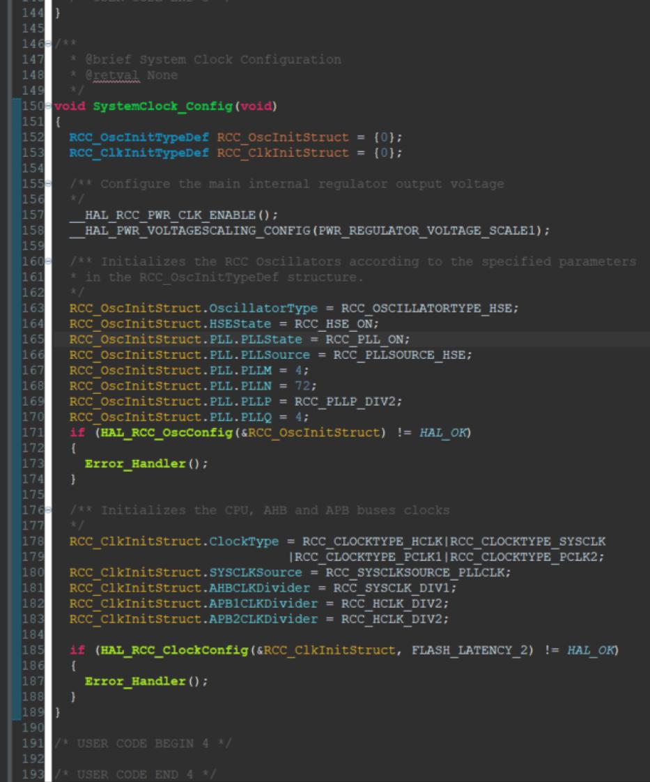
The firmware development process begins with the design phase, where
the
software architecture is meticulously planned.
During this phase:
- Programming Language Selection: The optimal language is chosen, considering the target platform, performance needs, and available development resources.
- Memory Allocation Strategies: Efficient memory usage is planned to ensure operation within hardware limits.
- Data Storage Solutions: Approaches to data management are decided to maintain data integrity and accessibility.
This design phase is critical, establishing the firmware's structure and ensuring scalability, maintainability, and robustness.The process then advances to the development phase, where the actual firmware code is crafted. Key activities in this phase include:
- Algorithm Implementation:Writing the core algorithms essential for the firmware’s functionality.
- Driver Development: Creating drivers to interface effectively with hardware components.
- Integration: Incorporating third-party libraries or APIs to enhance functionality.
Next, extensive testing and optimization is conducted, a vital stage before deployment. This phase entails:
- Code Optimization: Ensuring the firmware runs efficiently by eliminating redundant code.
- Timing and Scheduling: Fine-tuning timing parameters and task prioritization to ensure component synchronization.
- Communication Protocols: Verifying reliable communication between components to prevent data loss or delays.
- Power Management: Reducing power consumption by adjusting clock speeds and voltages, and implementing power-saving modes like idle or sleep.
- Error Handling and Recovery: Establishing robust error detection and recovery mechanisms to minimize system disruptions and ensure quick recovery.
Our firmware development services empower your hardware, allowing you to achieve maximum functionality, seamless integration, and efficient control over your devices. We offer various solutions, from creating low-level firmware to modifying and debugging existing firmware for optimal performance.
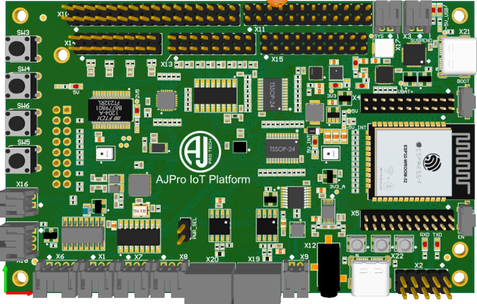
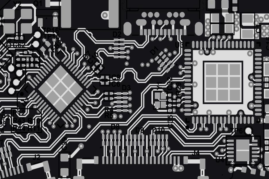
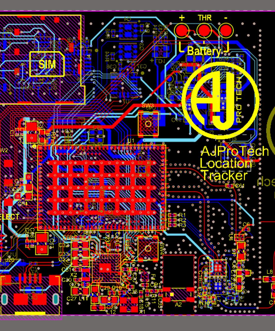
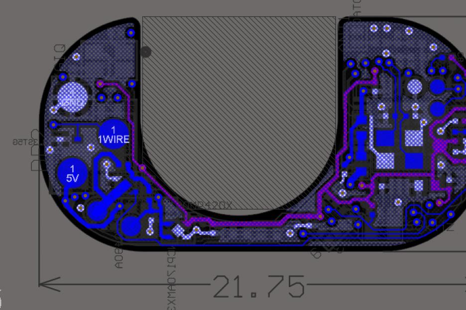
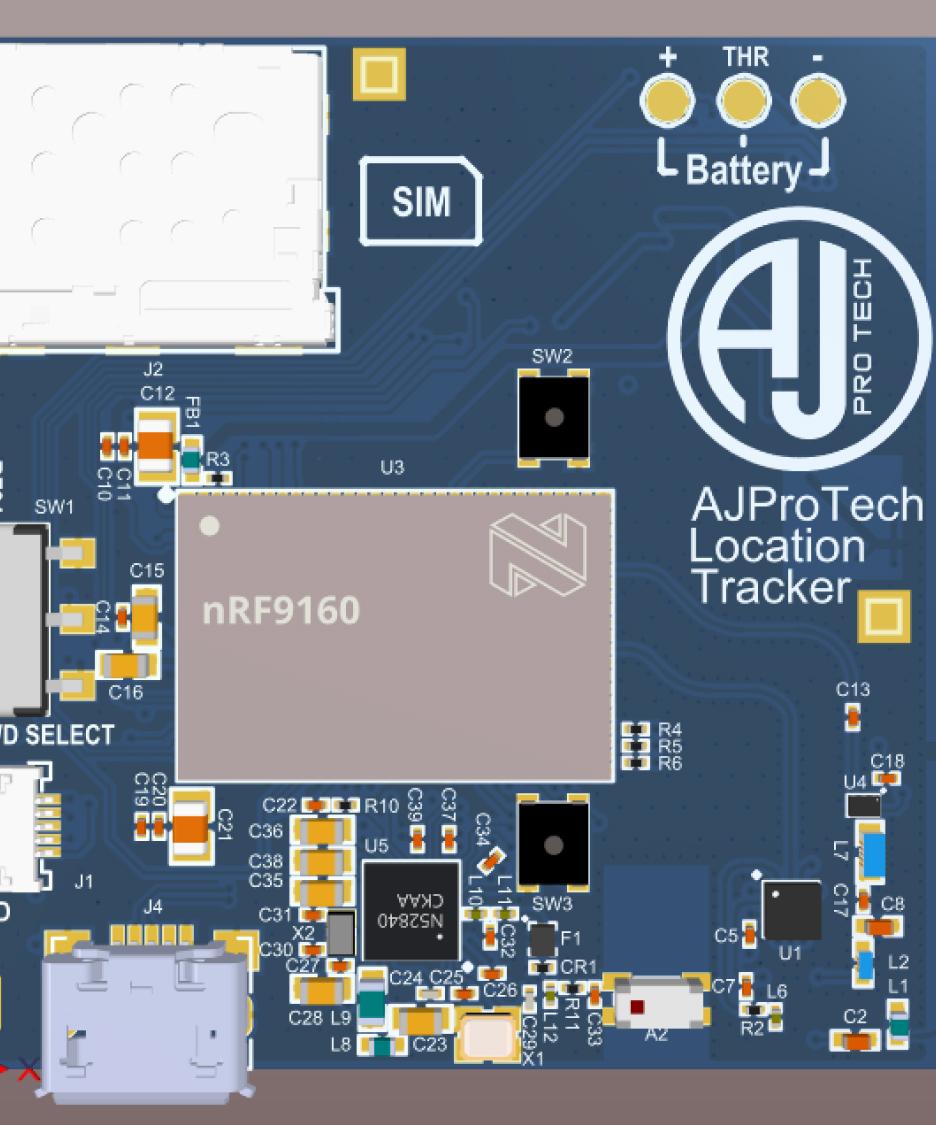
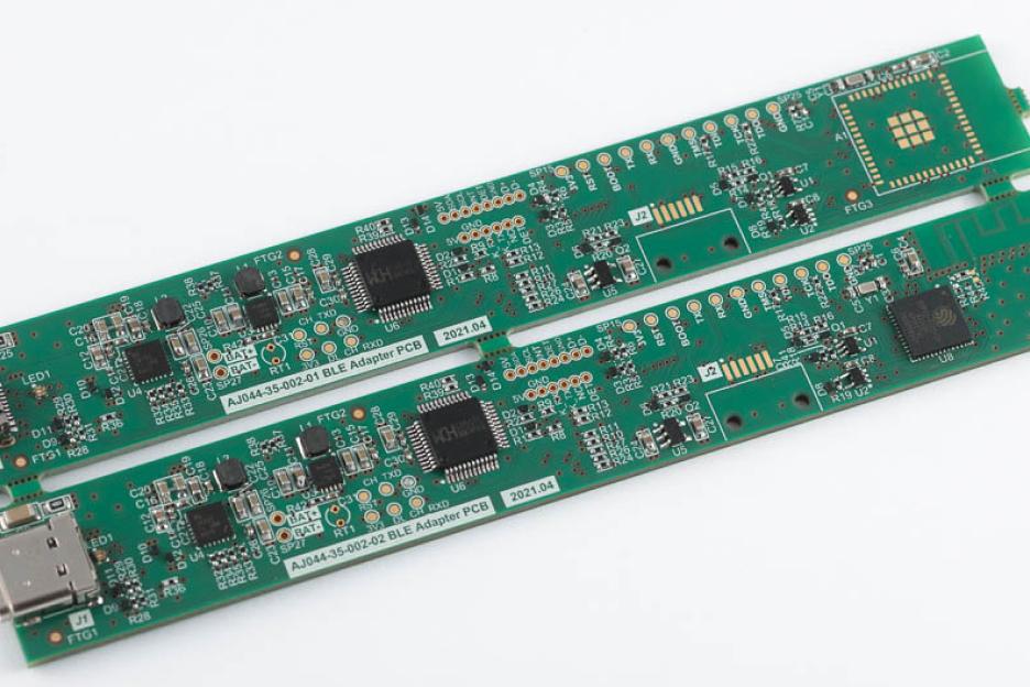
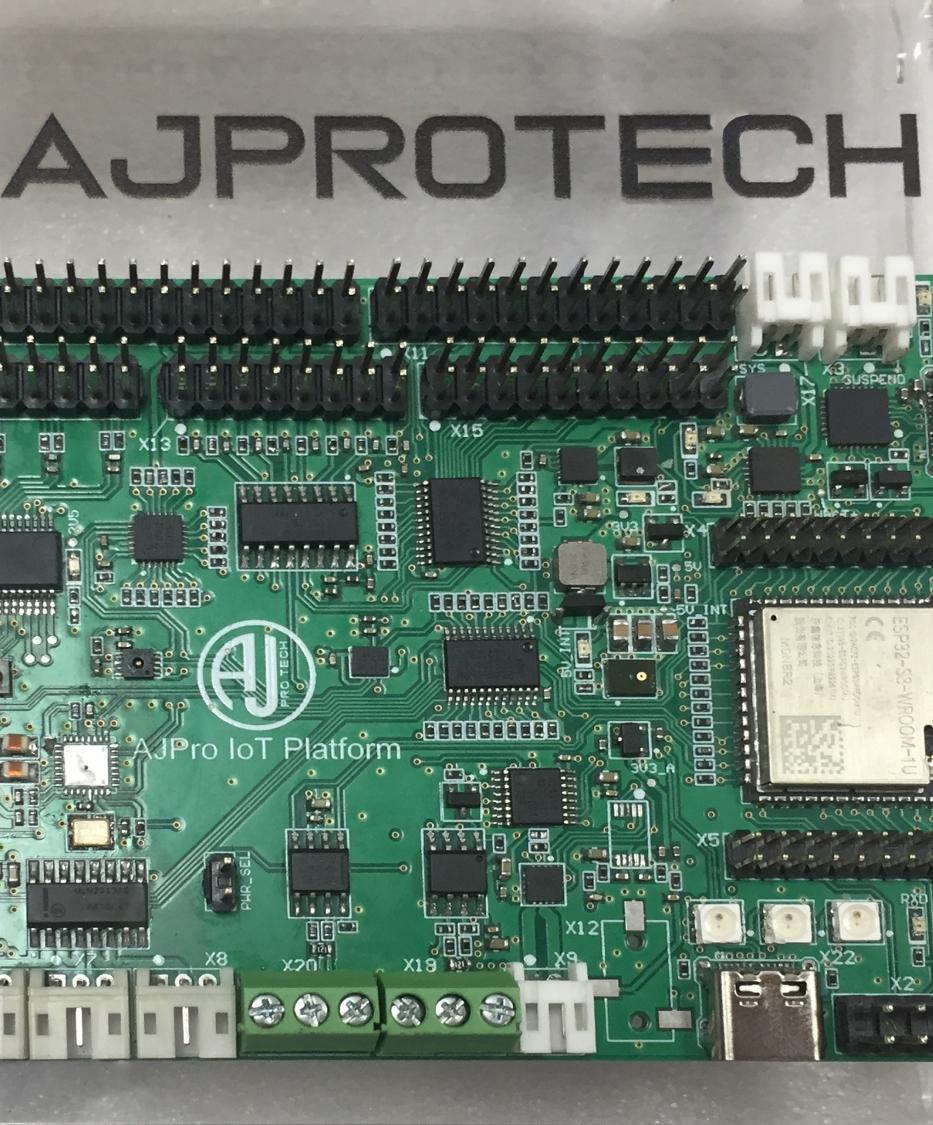
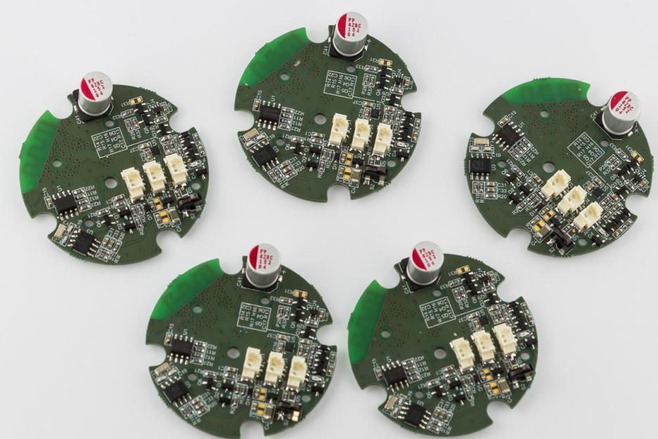
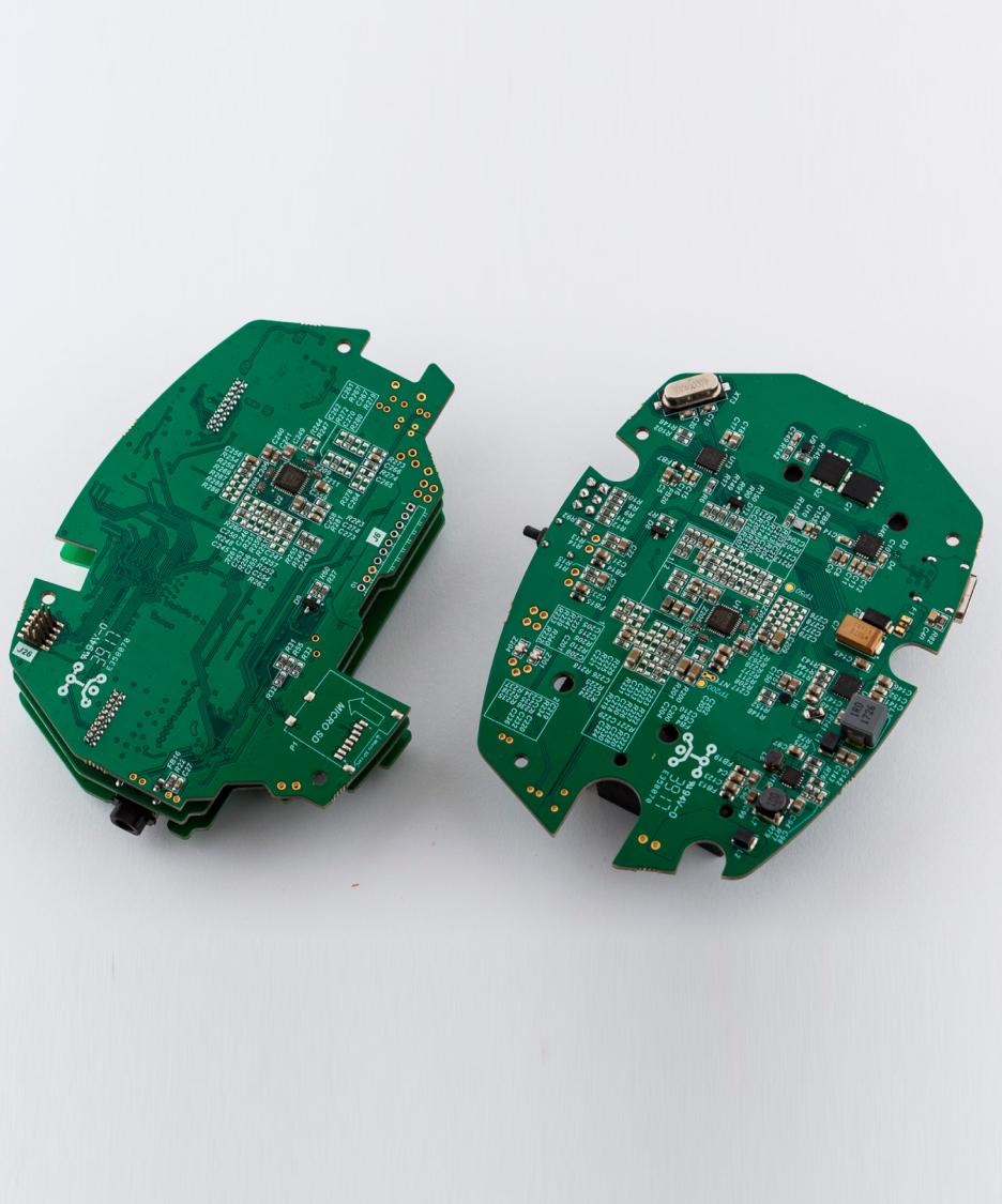
PCB DESIGN - Engineering prototypes
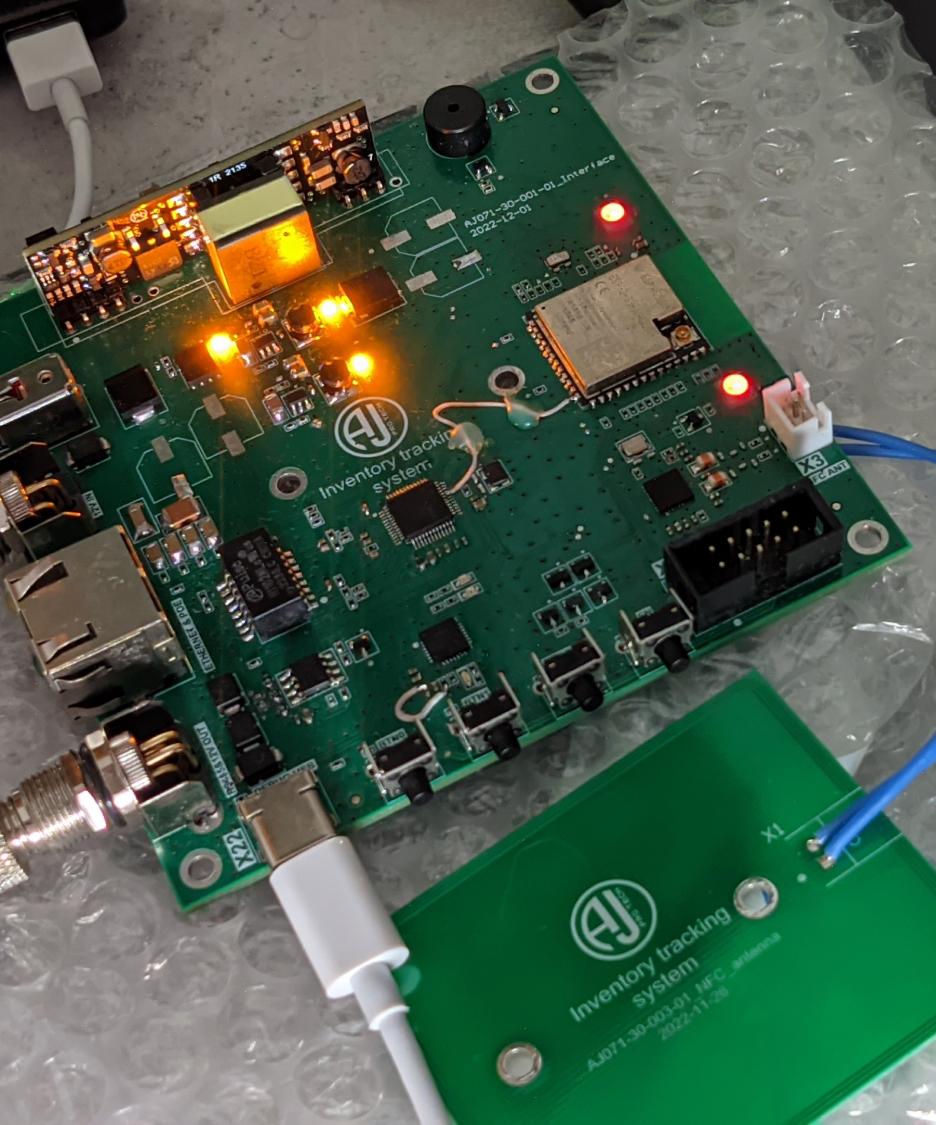
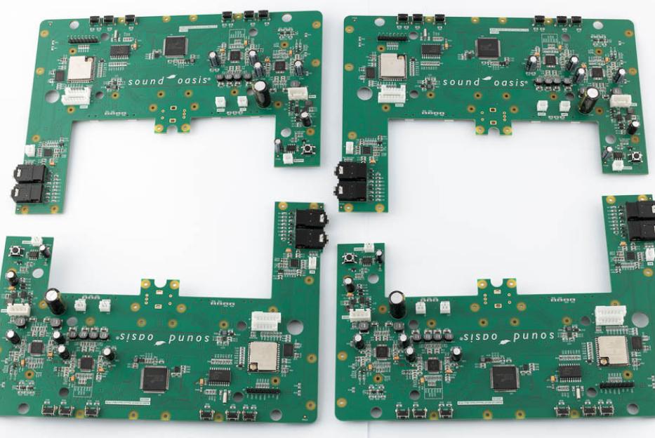
Engineering prototypes typically begin with custom-made PCBs (printed circuit boards). These custom PCBs are designed specifically to meet the unique requirements of the prototype, allowing engineers to test and validate their concepts effectively.
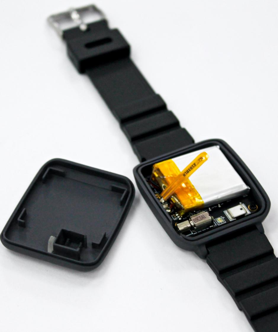
A Printed Circuit Board (PCB) is designed to support electronic components such as resistors, capacitors, diodes, and integrated circuits. It provides a physical platform for the components to be attached to, allowing them to be connected and function together. The PCB design is usually created using specialized software, such as CAD tools. Once the PCB is fabricated and firmware is flashed, it is integrated with other hardware elements and software components, enabling the complete prototype to be assembled.
Throughout the manufacturing process, quality control is always in place to ensure that the PCB meets specifications and high industry standards. This includes testing for thickness and width measurements, solder mask printing quality, misaligned or damaged tracks etc.
PCBA production
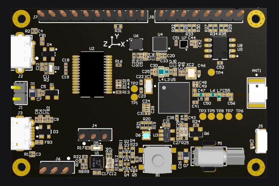
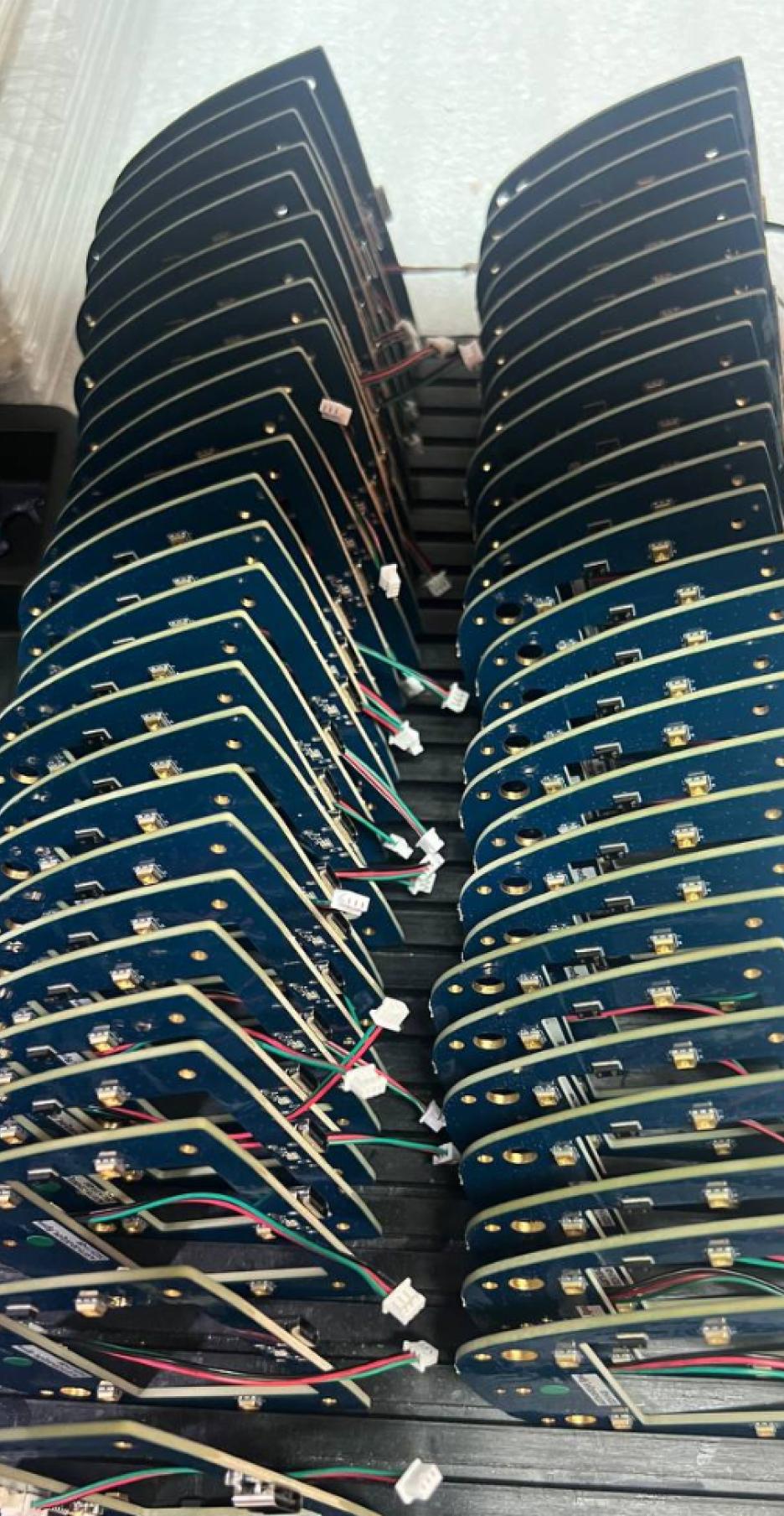
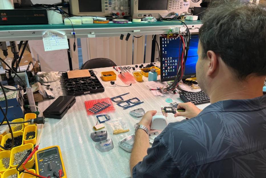
PCBA (Printed Circuit Board Assembly) production involves assembling electronic components onto printed circuit boards. This process is typically carried out by a dedicated team of engineers, especially during product development when manual assembly is common. Manual assembly allows for precise placement of custom-made components and offers flexibility for small batch or low-volume production.
The assembly process includes two main steps: placing components and soldering. For Surface Mount Devices (SMDs), flux is applied to the pads, and components are carefully placed using tweezers or a pick-and-place tool. Through-hole components follow a similar placement method.
Soldering joins the components to the PCB by melting solder paste between the component leads and pads. A soldering iron is used to heat the paste, creating a strong connection.
We prioritize careful handling of components and maintain a clean environment to avoid errors. Our engineers use proper techniques and high-quality tools to ensure the best results.
PROTOTYPE ENCLOSURE
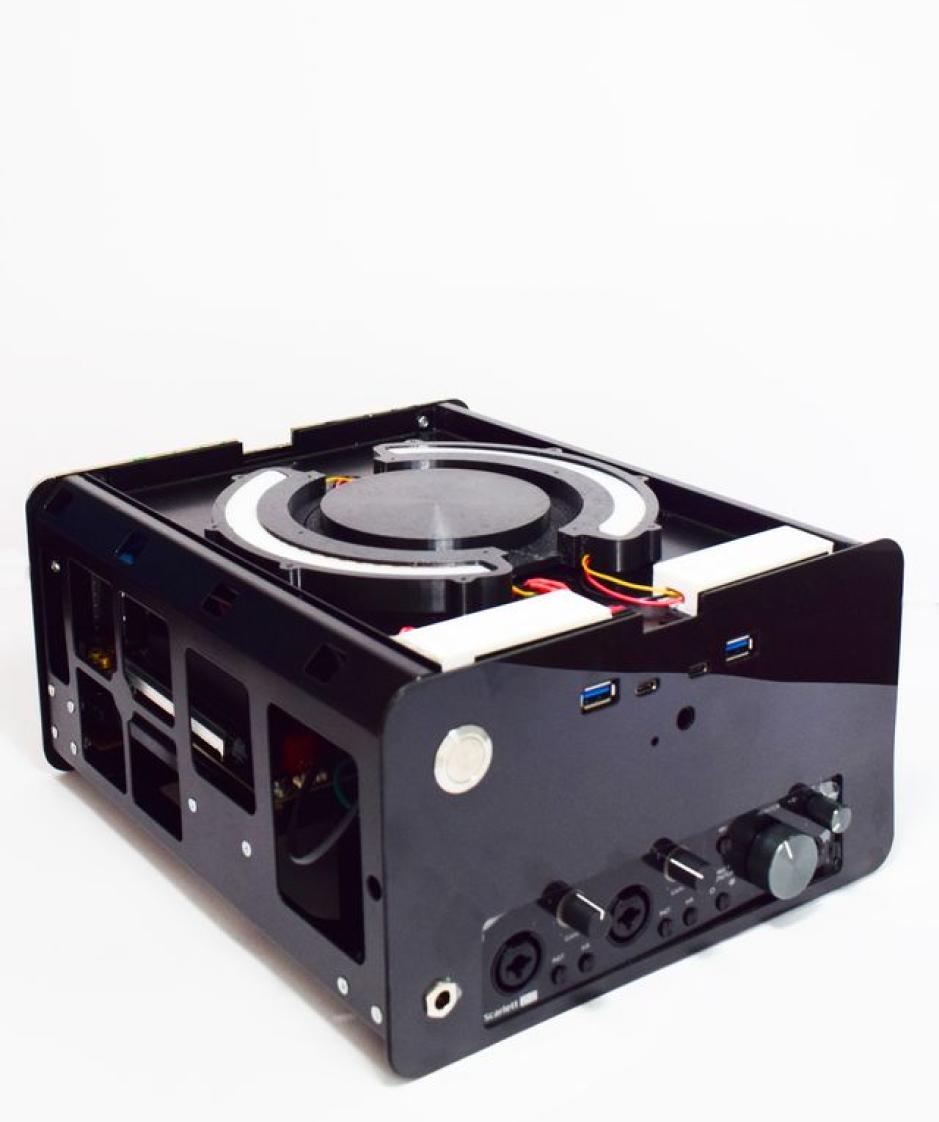
The relationship between form and function in design is often a delicate balance. On one hand, designers strive to create devices that are aesthetically pleasing, emphasizing particular shapes and styles. On the other hand, engineers impose requirements based on durability, complexity, ventilation, heat dissipation, and other practical considerations.
Material selection plays a critical role in this equation. It cannot be compromised, as it significantly impacts the overall user experience. For instance, materials that are prone to scratches or damage may not be suitable for devices that will be handled frequently. Conversely, materials that are excessively brittle may fail to withstand the stresses and strains of daily use. Moreover, certain materials possess specific properties crucial to the device's performance, such as thermal conductivity or electromagnetic shielding.
By thoughtfully selecting the appropriate materials, we can ensure that our device not only looks great but also performs its intended functions effectively. This harmonious integration of aesthetics and practicality is essential for creating a successful prototype enclosure.
3D printing and silicone molding CAPABILITIES
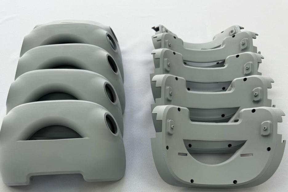
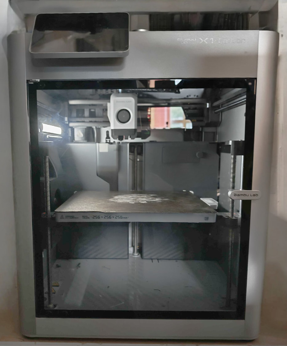
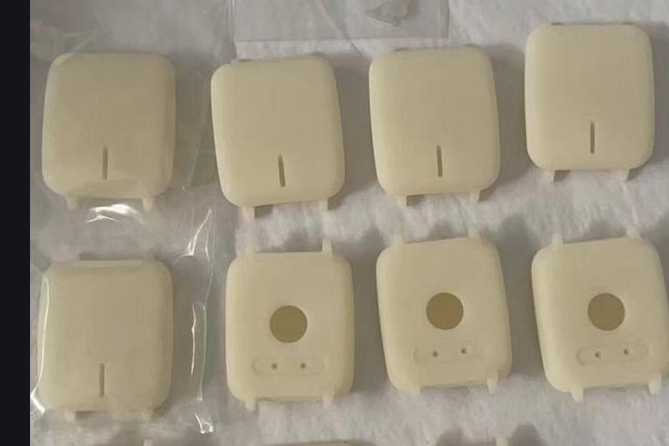
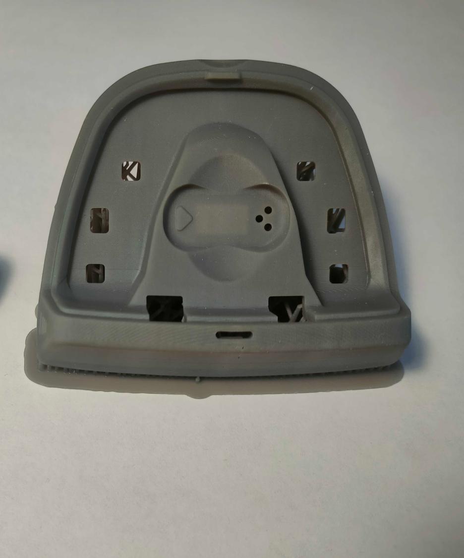
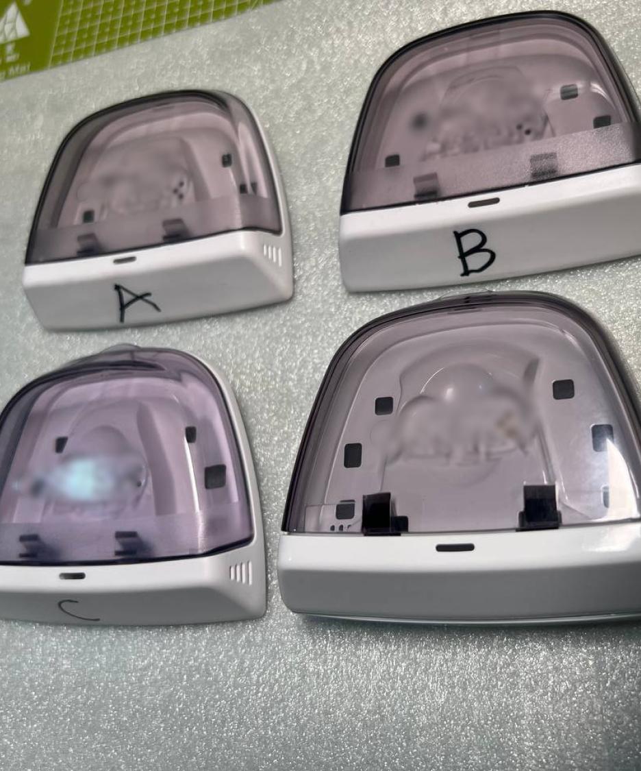
At AJProTech, we provide 3D printing services tailored to diverse industries. Our engineering team helps you choose the right 3D printing technology and materials to meet your needs and get your products to market faster.
Selective Laser Sintering (SLS) enables the creation of complex, high-quality parts with exceptional precision by fusing polymer powder with a laser. Known for producing durable components with excellent surface finishes, SLS is ideal for aerospace, automotive, and healthcare applications.
Stereolithography (SLA) delivers high-resolution parts with intricate details and smooth finishes by curing liquid resin with a laser. It's perfect for prototypes and detailed models, excelling in applications where precision and visual appeal are essential.
Fused Deposition Modeling (FDM) crafts parts using various thermoplastics, resulting in highly durable and robust components. This strength makes FDM perfect for applications requiring resilience, such as creating jigs and fixtures for work-holding tasks.
Multi Jet Fusion (MJF) 3D printing is an excellent choice for producing precisely detailed parts with consistent mechanical properties at a rapid pace. It excels in creating functional prototypes and is well-suited for short to mid-volume production runs, including bridge manufacturing.
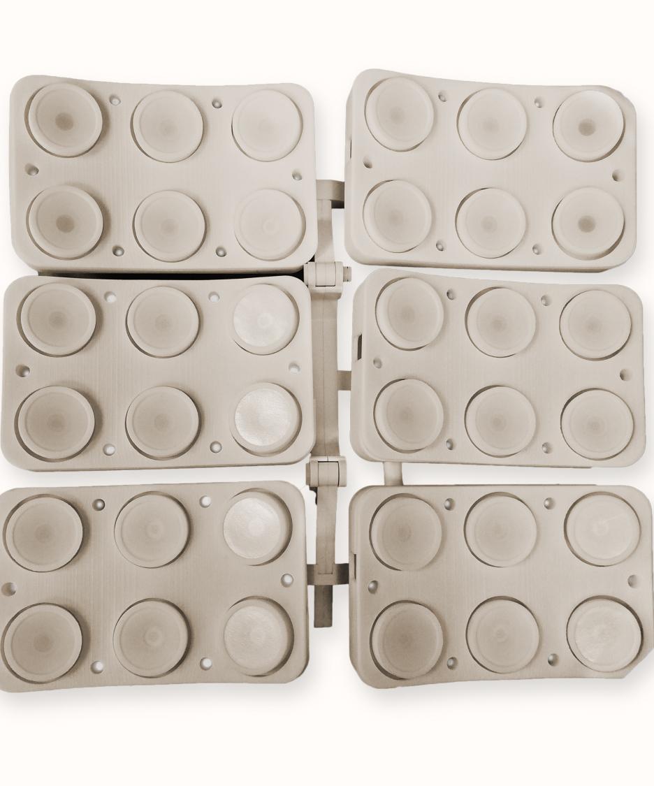
Silicone molding is a great decision for prototyping and low-volume production, especially in IoT device development. Its flexibility and durability allow for capturing intricate details, making it perfect for complex geometries. It's used to create prototypes or mass-produce components with consistent quality.
Let's talk about your project
PROTOTYPE ASSEMBLY
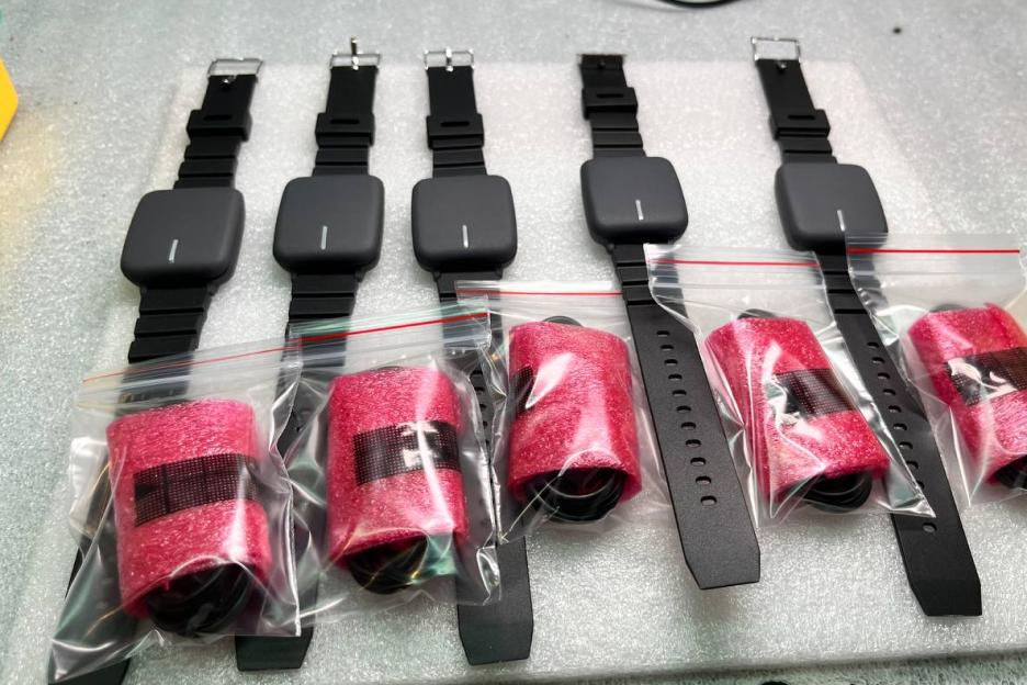
After planning and designing phases done right - prototyping phase went easy and all stated goals of the device were achieved and proven. This is where the team's hard work and creativity come together to bring the product to life, and it's often the most exciting moment in the development process.
A well-assembled prototype is a crucial step in ensuring that the final product meets partner’s expectations and customer needs.
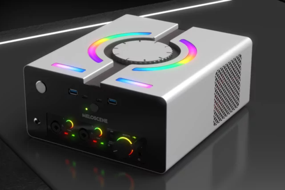
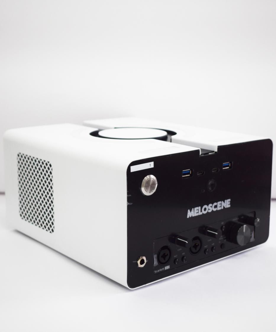
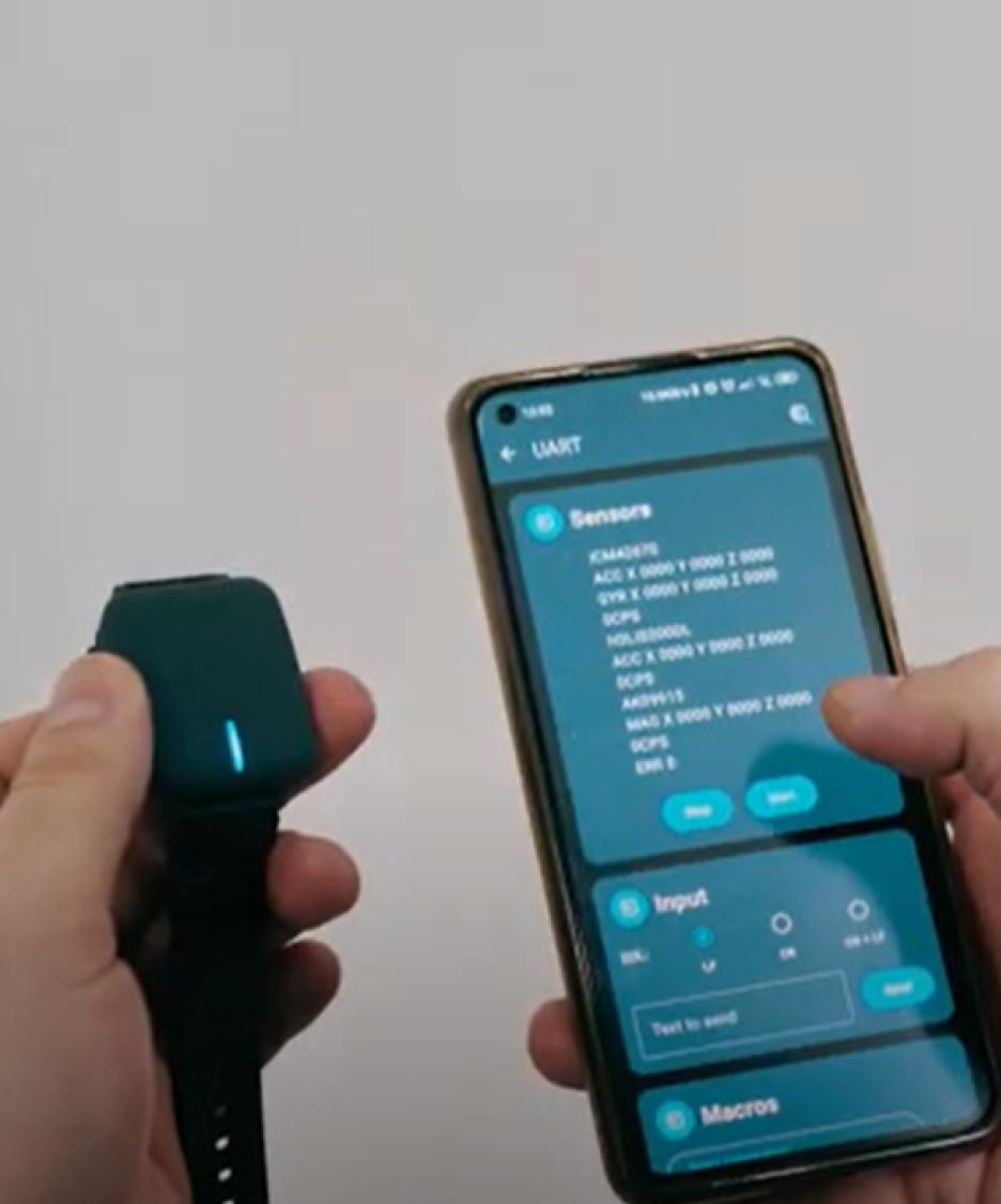
Meloscene SceneKey prototype assembly
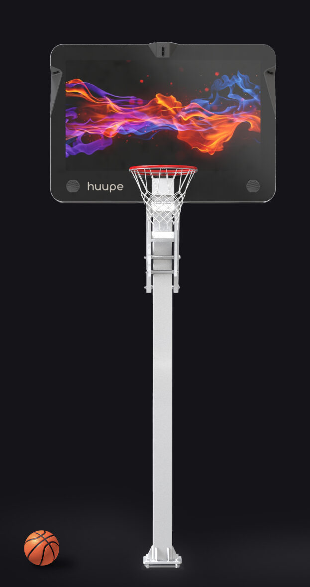
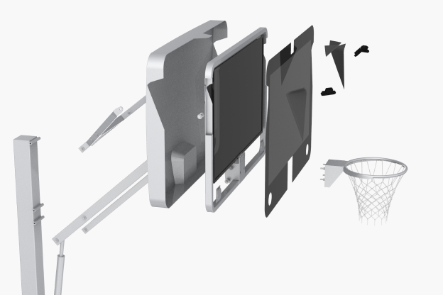
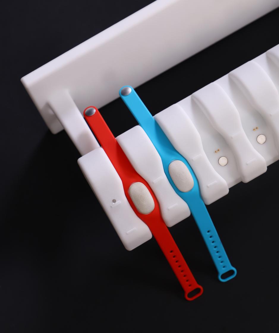
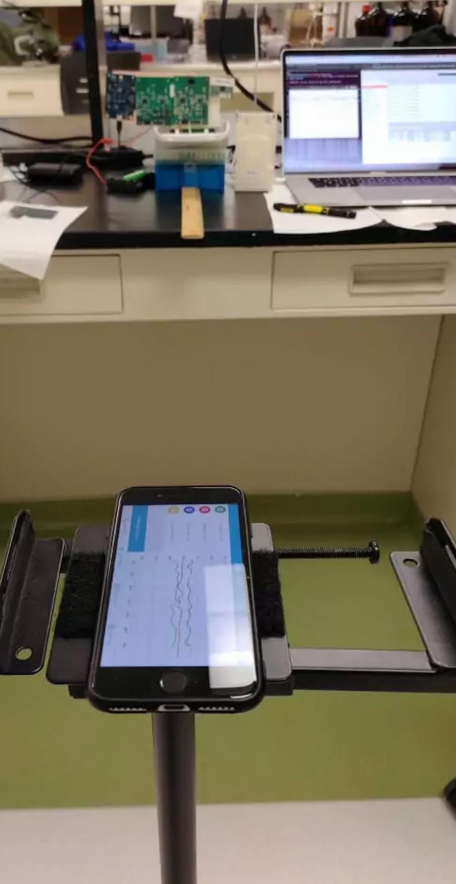
Huupe prototype assembly
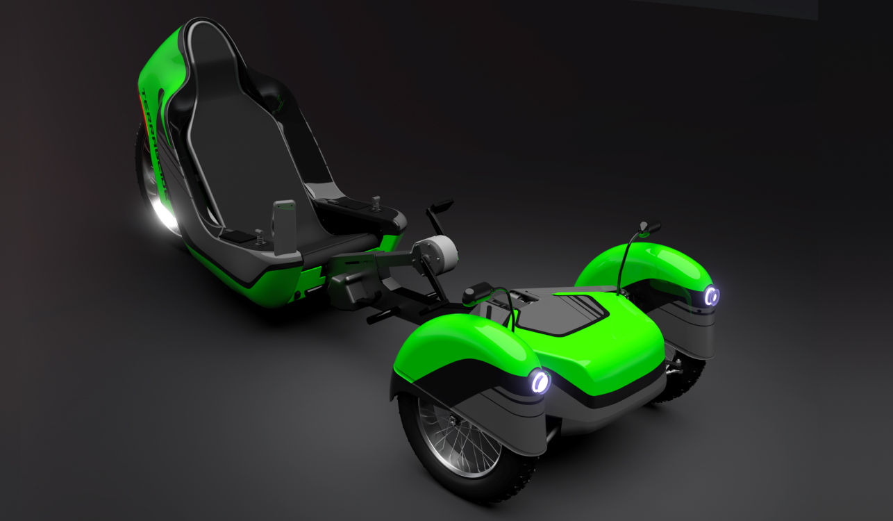
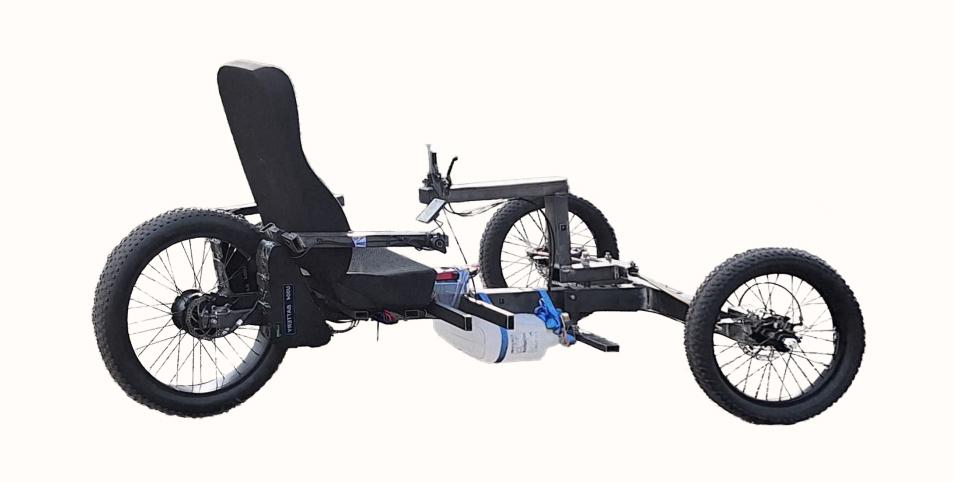
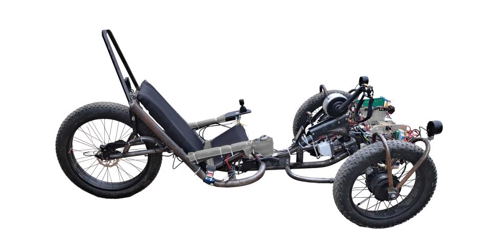
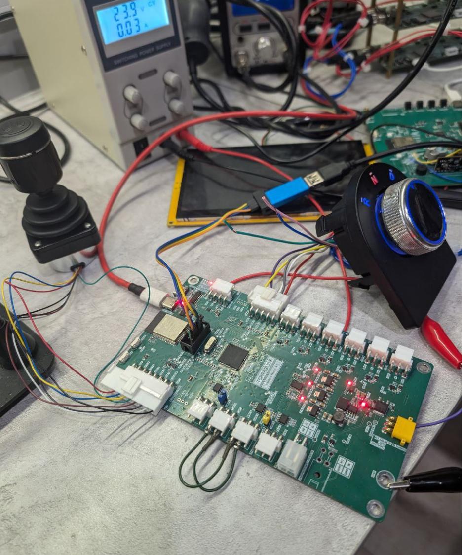
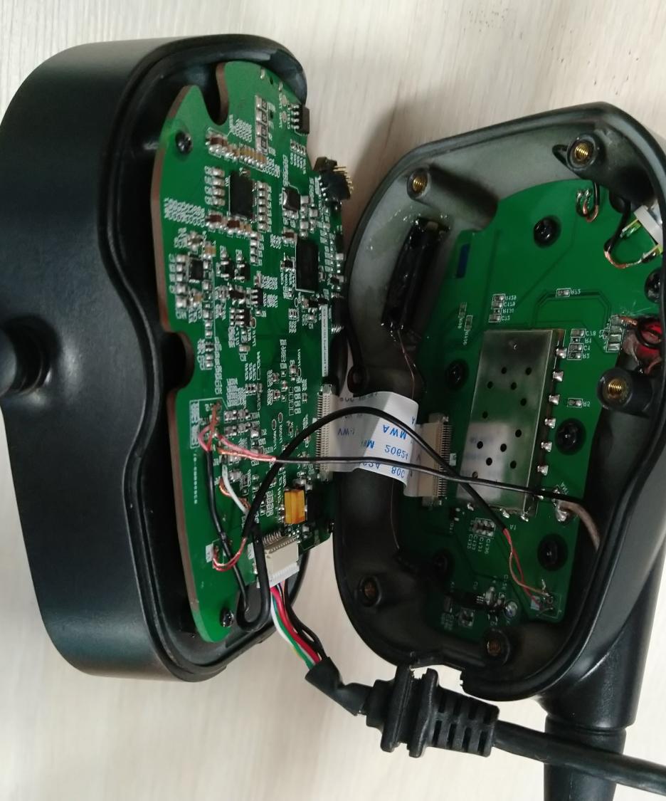
Terraglide. How we built this
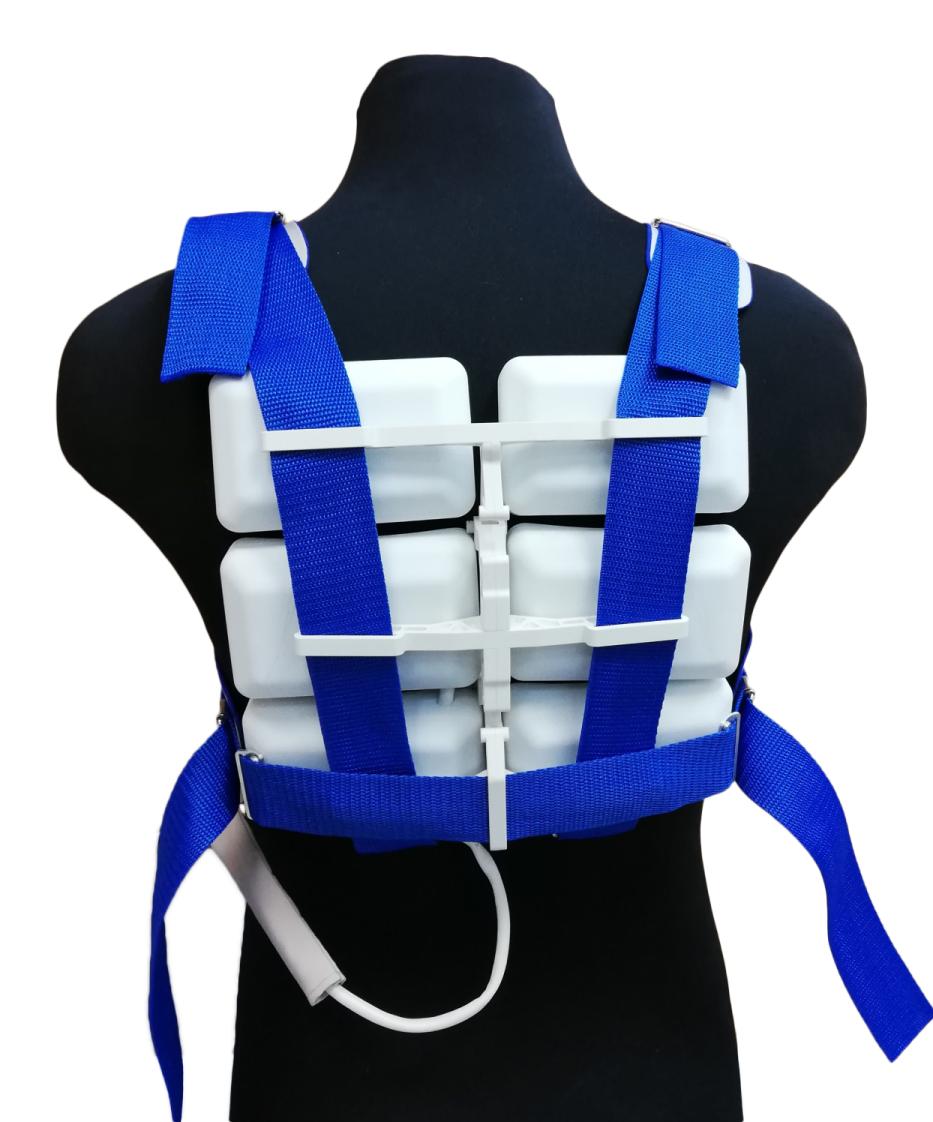
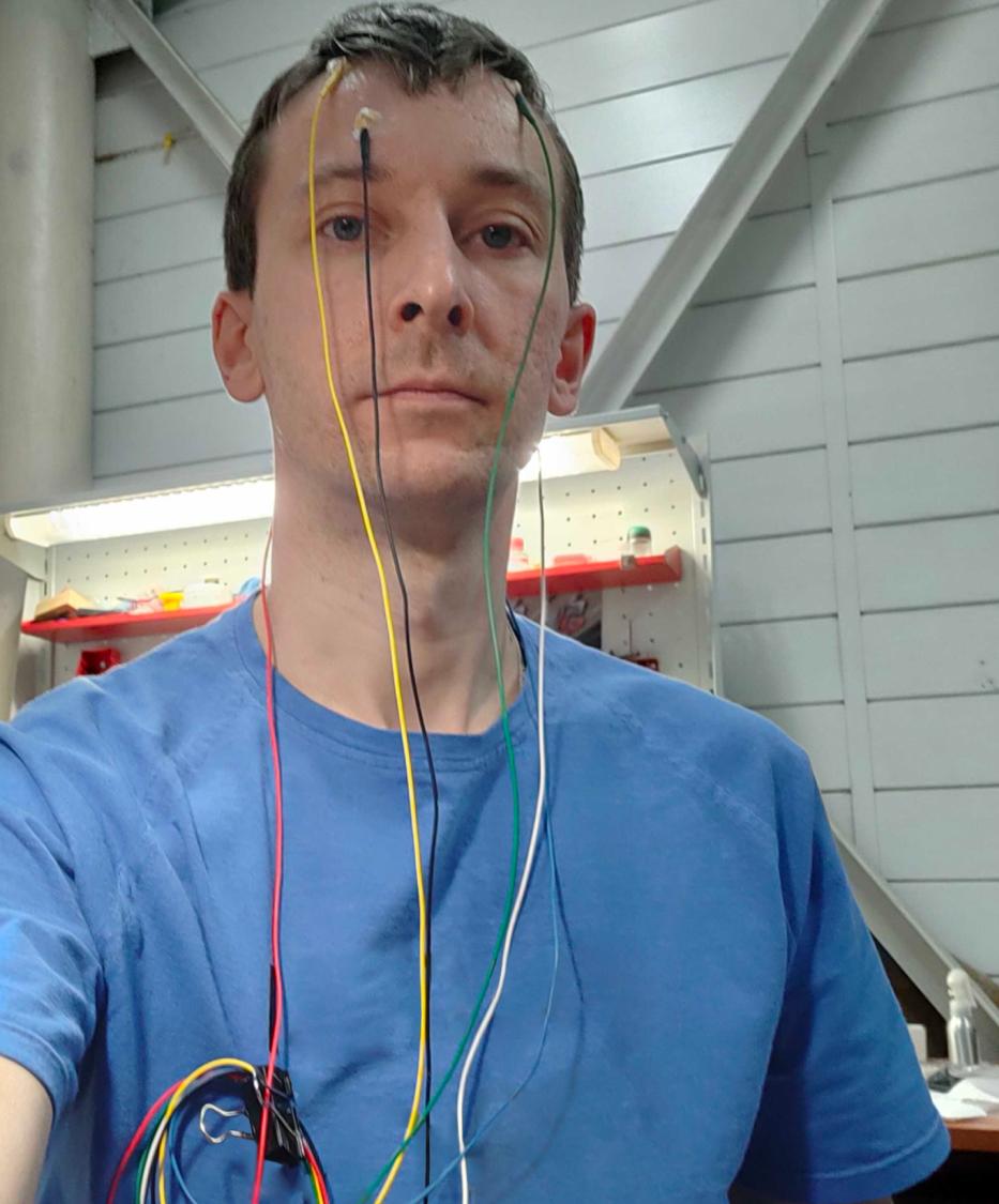
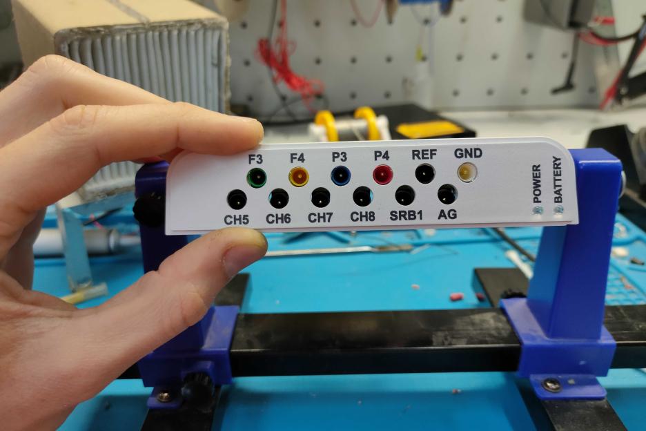
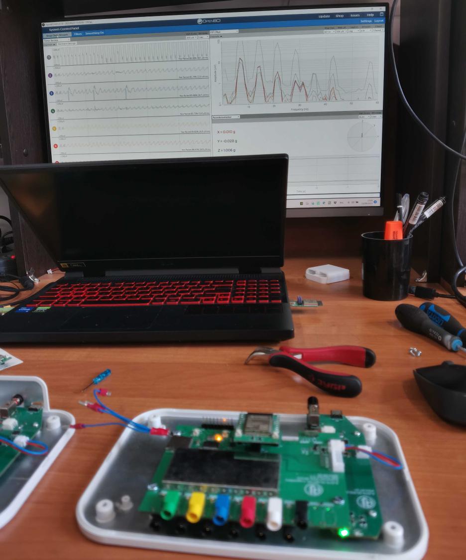
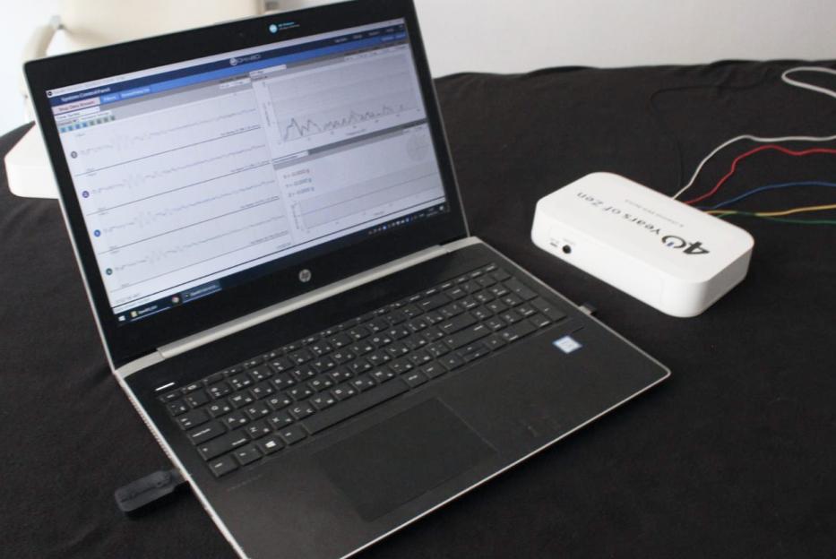
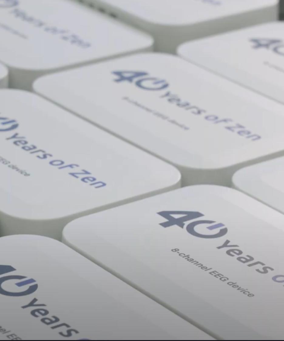
Neurofeedback EEG device assembly. 40 years of Zen
HARDWARE PRODUCT DEVELOPMENT: Prototypes Testing
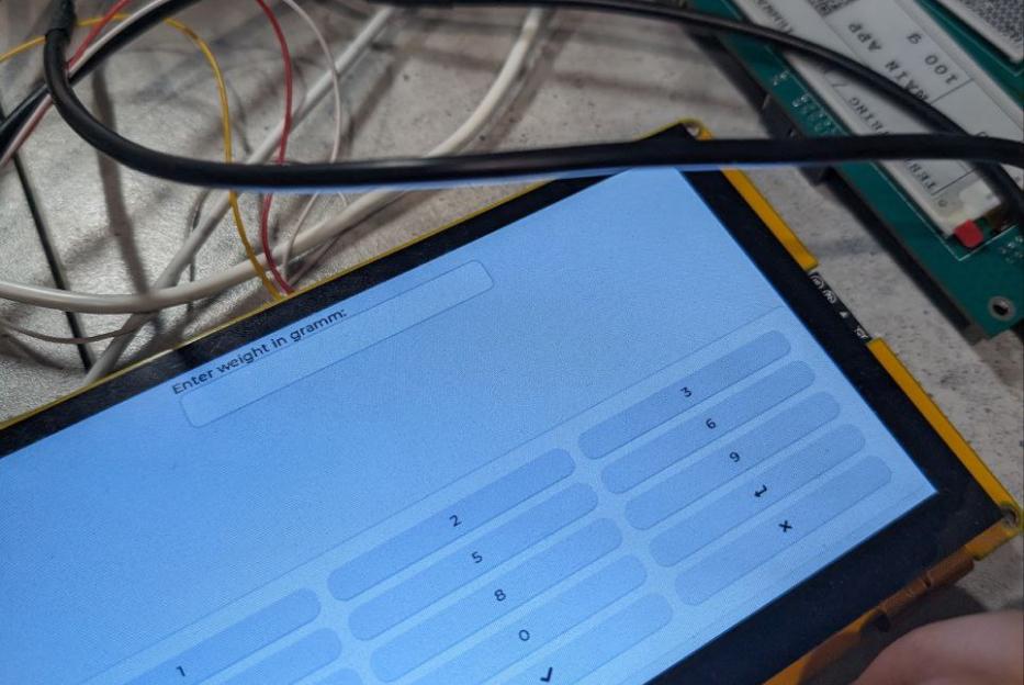
Prototypes are subjected to various tests to assess functionality, durability, usability, and compliance with relevant standards. This may include both qualitative and quantitative assessments, as well as simulations and real-world testing environments.
Based on test results, prototypes are modified to address flaws and enhance features. Once approved, the prototype is prepared for shipment to the customer.
ENGINEERING VALIDATION TEST (EVT)
After obtaining samples, the next critical step is to validate the product, referred to as the Engineering Validation Test (EVT). Typically, this involves either using existing engineering prototypes or creating a new set of prototypes as necessary. The core question to address during this phase is: “Does the product meet the functionality outlined in the Product Specification?”
Typical test to run:
- Functional
- Power
- Thermal
- EMI
Functional tests are:
- How does the device power up?
- Is all communication working?
- What's the power draw?
- The core functionality for the device is being tested here.
The EVT primarily focuses on testing the core functionality of the device. If the device features wireless connectivity, it is essential to assess Received Signal Strength Indicator (RSSI) and evaluate the communication range. It is advisable to test how many devices can operate simultaneously within the same vicinity. For instance, Bluetooth typically allows around five connected devices, so understanding device limitations is crucial when designing for wireless capabilities.
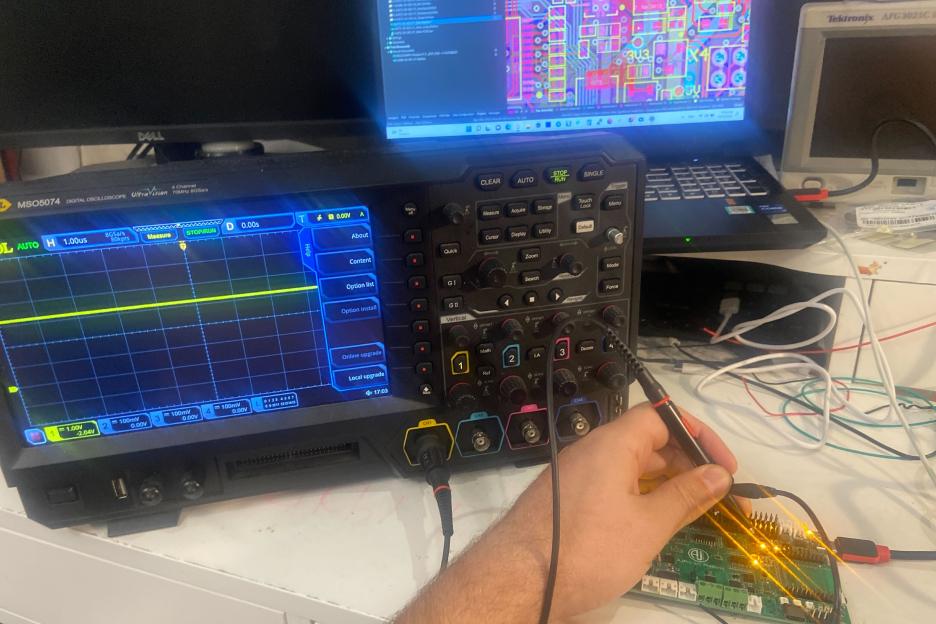
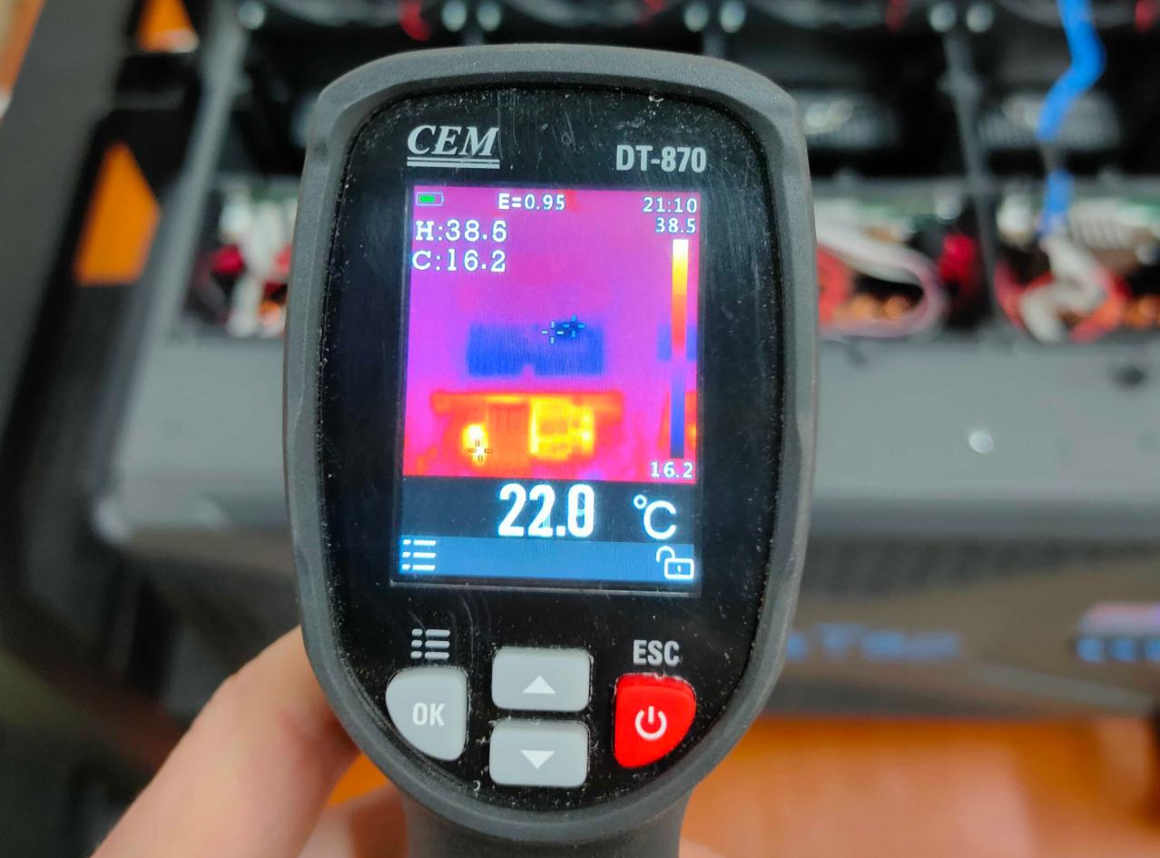
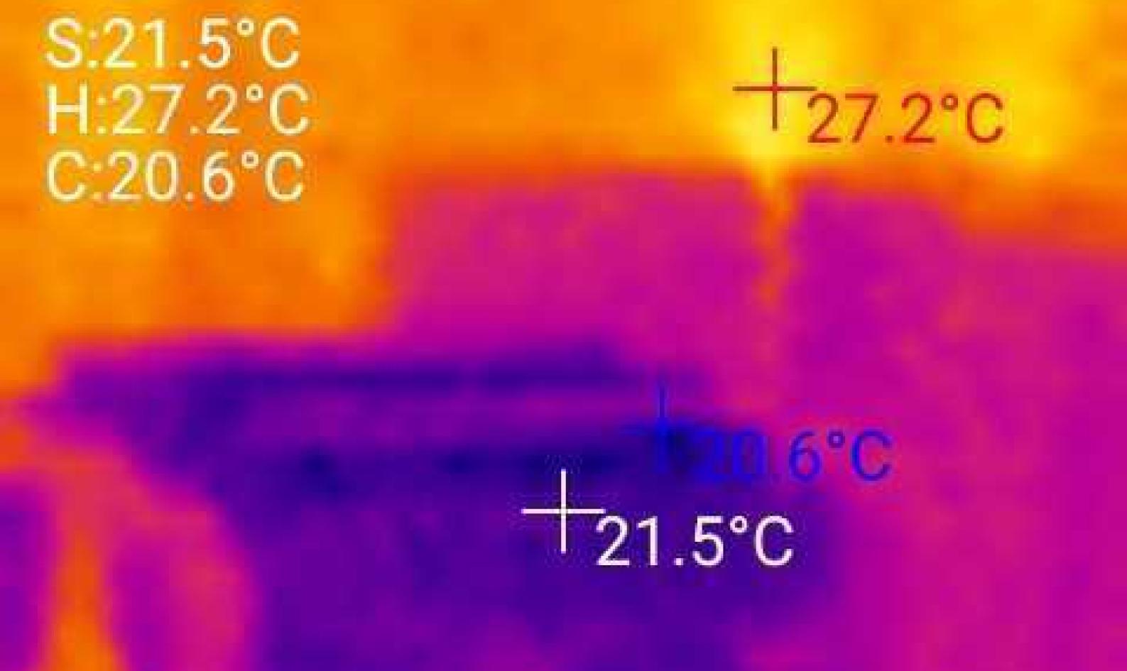
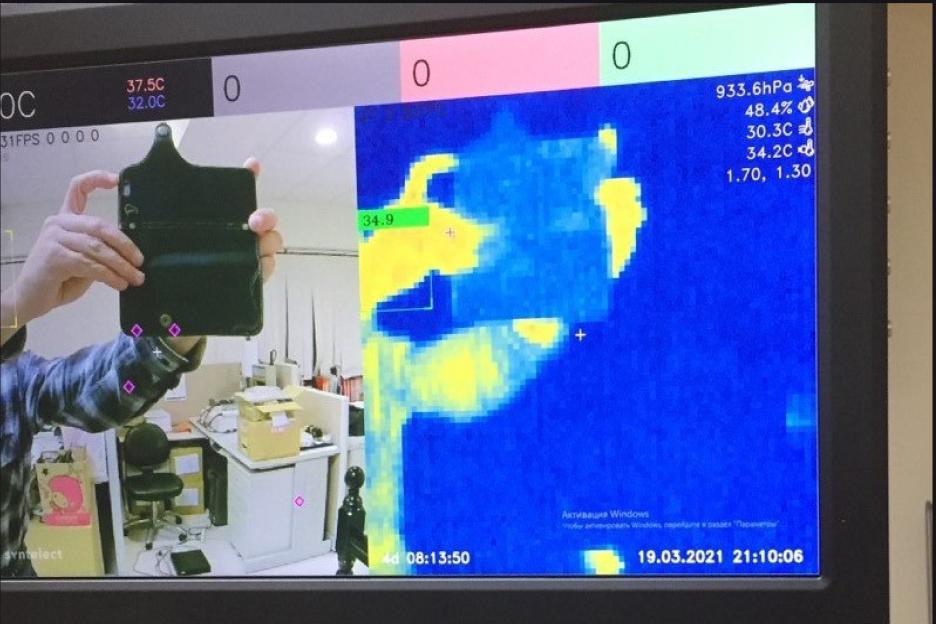
Another valuable recommendation is to utilize thermal cameras extensively during testing. A cooler-running product tends to be more reliable, so it is imperative to perform thermal analysis at both the PCB and product levels. Identifying which parts of the design overheat will guide further improvements. Ultimately, reducing heat generation enhances device stability and longevity, making this testing phase worth significant investment.
During the EVT process, you should “lock” components; significant changes to component selections should not occur post-EVT. If necessary, an additional EVT iteration may take place, but anticipating changes later is not advisable. When collaborating with a Contract Manufacturer (CM), expect limited tolerance for modifications after this stage, so it is vital to secure your component database during EVT.
When assembling PCBs by hand, it is crucial to work in a well-lit environment and handle components with care to avoid damage. Employ proper soldering techniques, including controlled temperatures without excessive heat, and consider utilizing a PCB assembly jig or fixture to stabilize the PCB during assembly. Ensure precise component placement by using a flux pen or liquid flux on the pads, applying gentle pressure while positioning components. Maintain a clean and organized workspace to avoid contamination and errors.
DESIGN VALIDATION TEST (DVT)
As you advance from engineering tests (EVT), your goal by the end of the DVT phase is to have a set of finalized, validated and tested working engineering prototypes and to begin discussions with a contract manufacturer (CM). The DVT stage serves as the final validation before production commences. Here’s a breakdown of what typically occurs during DVT:
So what is typically done at Design Validation Test (DVT):
- Final Validation: Confirm that the product meets all specified requirements.
- Selection of Contract Manufacturer (CM): Choose a CM that will be responsible for assembling the units.
- Design for Manufacturing Optimization (DFM): Finalize mechanical designs to ensure manufacturability.
- Finalization of Electronics and Firmware: Ensure that all software and hardware components are fully integrated and functional.
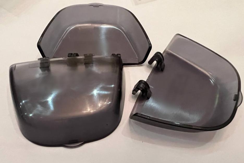
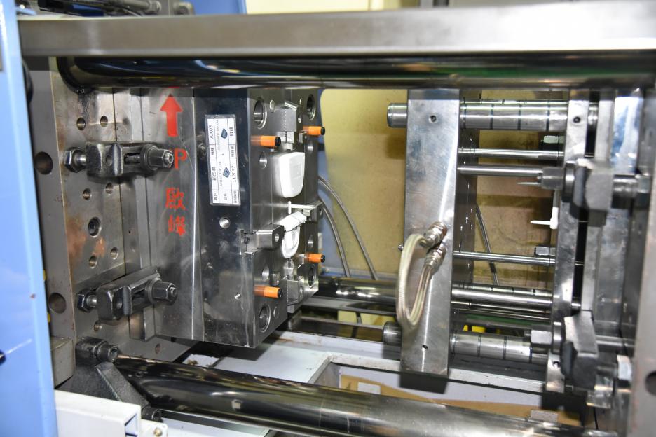
- Tooling Preparation: Complete any necessary tooling, including first-shot tooling, which the CM undertakes to produce key components and an initial batch of 50 - 100 units.
The major question you answer at the end is: “does the product meet all requirements?” Functional, cosmetics and environmental.
At the end of DVT, you’re expected to have anywhere from 10 to 50 prototypes which need to look good and perform as your final product even though they’re not revenueable yet.
As your production volume scales up, you need to invest time in scripting. Don’t test each individual unit separately, create a script typically in Python to automate some of your testing. This is going to be used a lot at a production stage. This is the time when you start investing time and money into this testing process.
Typical tests you run at the end of DVT:
- Functional - including usability
- Performance - does the product meet all the functions you define
- Climatic - how device operates into into cold and hot conditions
- Reliability - stress testing
- Mechanical, shock, vibration
- Mean time between failures (MTBF)
- Electromagnetic compatibility (EMC) test
- Compliance testing (FCC, UL, CE)
You might even go as far as doing some pre compliance testing so FCC and UL might start here.
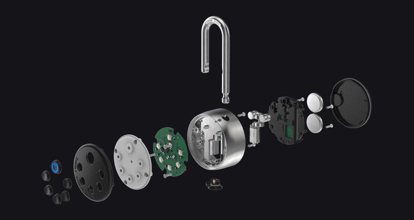
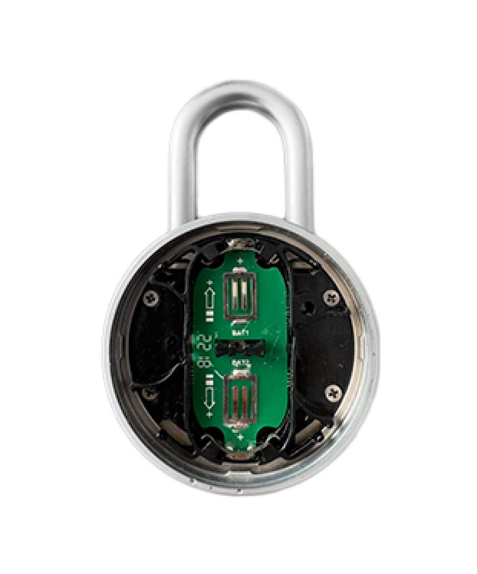
In the case study of the smart Bluetooth padlock project, one of the core features is: how many times we can press the buttons and put the shackle out before it fails. So we program the CNC machine at the factory to physically press the buttons and extract the shackle from it. It was running for non-stop before we first saw any sort of failure and adjusted our design. Don’t skip this phase, don’t produce your badge and don’t wait till it’s too late.
Climatic testing. Do thermal cycling. How the device performs when you cool it down and you heat it up, those are the words for the product. Test extreme conditions - the coolest and hottest for the product. It can be done in a thermal chamber. If you don’t have one, you can go to the local testing facility and they definitely have those chambers available for rent.
Moreover, most products intended for sale in the U.S. must pass EMC and EMI testing. For audio products, it's crucial to assess microphone performance. Selecting a CM with prior experience in these tests can simplify the process and significantly lower testing costs.
PRODUCTION VALIDATION TEST (PVT)
After the DVT stage confirms that the product performs as expected, the next step is the PVT - Production Validation Test. This final validation phase ensures that manufacturing processes are capable of consistently producing the product with the required quality before mass production begins. Successfully completing the PVT verifies that the product is ready for full-scale production.
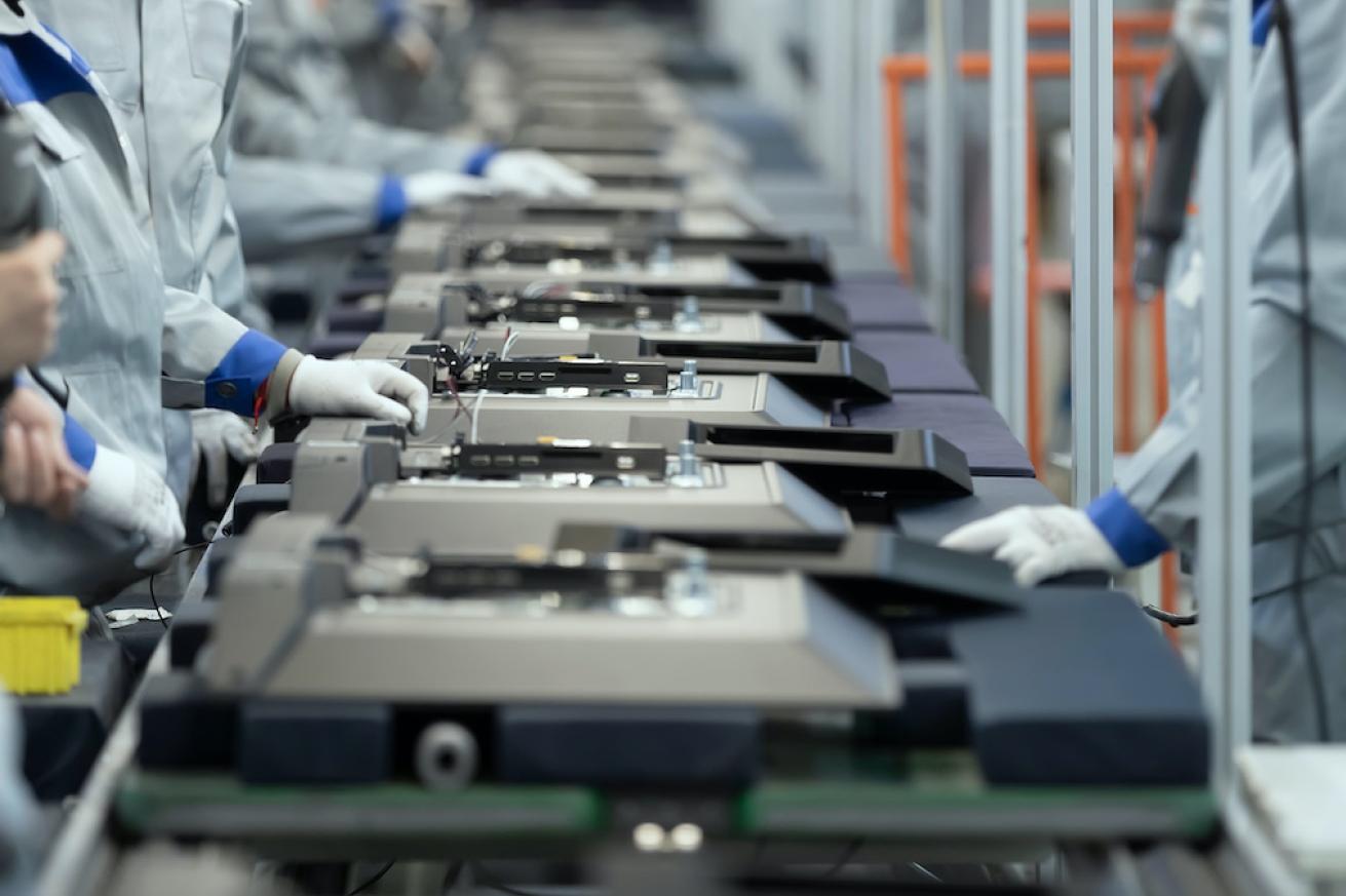
During the PVT phase, the factory prepares processes for mass production, creating the first sellable units. Typically, around 10% of the initial batch is manufactured, so for a target of 5,000 units, the PVT produces approximately 500 units. The focus shifts from development to production, involving supply chain optimization, component sourcing, functional testing, and creating test jigs for analysis.
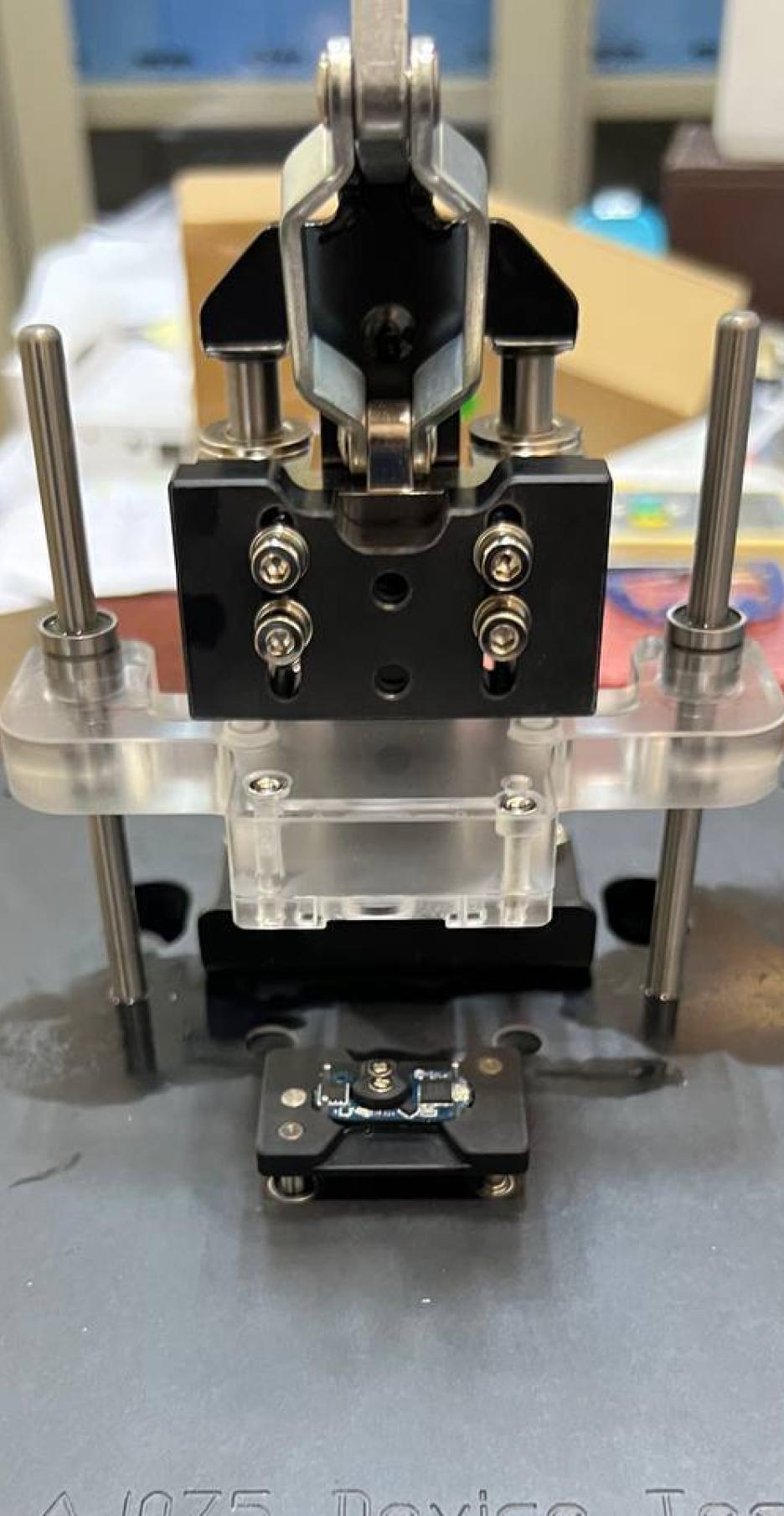
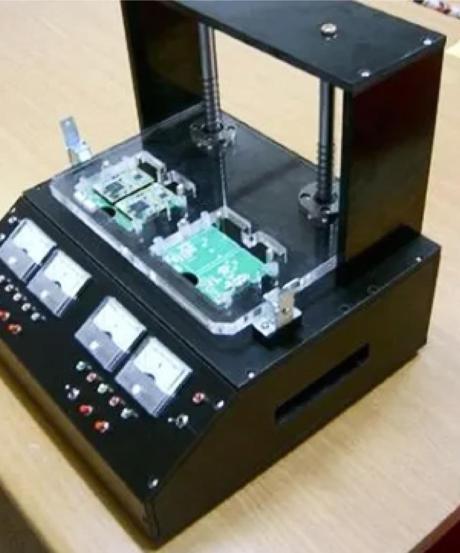
The supply chain is a driving factor during this stage, requiring the factory to determine where to purchase each component, understand lead times, and prioritize spot buys, which are costly, versus planning orders based on lead times. The factory also handles the creation of testing jigs and fixtures, programming the device, and testing it. The cost for a testing jig typically runs into several thousand dollars at this stage.
And at the end, you have the first product which can be sold, which can be sent to customers and which can be officially used for your compliance testing.
At this step, our team takes on the role of an overseer and consultant for our clients. In this capacity, we ensure that the work of the Contract Manufacturer is carried out to the highest standards and in line with the client's specifications. Our approach involves double-checking the work of the Contract Manufacturer at every stage of the project to identify any potential issues or areas for improvement. If necessary, we intervene to resolve any problems and ensure that the project remains on track. Our ultimate goal is to provide our clients with the peace of mind that comes from knowing that their project is being handled with the utmost care and attention to detail.
MASS MANUFACTURING
Mass production typically starts with an order of 5,000 units or more. During this phase, failure and yield analysis help determine how many units are not performing as expected, and the contract manufacturer (CM) plays a key role in maintaining a low production failure rate.
Regarding minimum order quantity (MOQ), different CMs may require anywhere from 5,000 to 10,000 units. Most CMs prefer to see at least $1,000,000 in bill of materials (BOM) for production. For example, if your product costs $200 to manufacture, 5,000 units would total $1,000,000. Conversely, if the unit cost is $100, you would need at least 10,000 units to meet this financial benchmark.
In terms of shipping, air freight is generally impractical for most products due to high costs, with the exception of major companies like Apple. Instead, plan for sea shipments, which typically take about four weeks from China to U.S. ports, such as Long Beach.
And when you do mass production, you no longer air-ship products. The only company that air-shipping their products is Apple with the iPhones. You plan your production in a way that you can afford time for sea shipment. It’s approximately 4 weeks from China to their port in the US, typically, it’s Long Beach for the West Coast.
Building IoT Products: A Guide from AJProTech Founder
Looking to create a custom IoT device? A comprehensive product development plan is crucial. In this video, AJProTech founder and CEO, Alex Gudilko, offers expert guidance on the entire process. Learn about securing funding, effectively designing, and transitioning your device from concept to mass production. Whether you're starting with an initial idea or preparing for market launch, Alex shares valuable advice to help you navigate each phase of IoT product development successfully.
What clients say about AJProTech
AJPROTECH Crafts World-Class Products
As an award-winning studio, we focus on creating projects that combine strong design with practical engineering. Our work has been recognized globally for its balance of innovation and functionality. We partner closely with clients from concept to final product, making sure each design is both visually appealing and practical, durable, and user-friendly. Our goal is to develop products that meet real needs and set a standard for quality in the industry.
Frequently asked questions
What is hardware product development?
Hardware product development is the process of transforming an idea into a tangible, market-ready product. At AJProTech, it includes every step — from research and feasibility studies to design, prototyping, testing, and mass production. Our cross-disciplinary team ensures each stage is optimized for performance, cost, and manufacturability.
What is the lifecycle of hardware product development?
The typical lifecycle follows these stages: Research → Early Prototypes (PoC, EVT) → Design Validation (DVT) → Production Validation (PVT) → Mass Production. AJProTech manages the entire process, ensuring reliability, scalability, and high-quality results.
How long does product development take?
Hardware product development usually takes between 12 and 24 months, depending on complexity and production goals. AJProTech accelerates timelines by using proven processes, in-house prototyping, and close coordination with manufacturing partners.
Why Hardware Prototype?
Prototyping allows teams to validate concepts early, identify design issues, and test usability before moving to production. AJProTech builds multiple prototype iterations — from “duct tape” mockups to functional units — ensuring that the final design meets user needs and compliance standards.
What makes AJProTech’s hardware development process unique?
Unlike most consultancies, AJProTech integrates industrial design, electronics, firmware, and manufacturing support under one roof. This full-cycle approach ensures faster turnaround, better quality control, and predictable outcomes — from concept sketches to mass production.
Can AJProTech handle certification and compliance testing?
Yes. We guide clients through compliance testing such as FCC, CE, and UL. Our team helps prepare documentation, conducts pre-compliance evaluations, and collaborates with certified testing labs to ensure smooth approval and market readiness.


