


Every printed circuit board starts its journey long before copper traces snake onto fiberglass. Without clear direction, circuit chaos is inevitable. The schematic comes first, transcribing system logic into an orderly list of symbols. This digital map ties together microcontrollers, capacitors, traces, and resistors.
Each line in the schematic ensures a signal gets from point A to point B, ideally with few detours. A detailed bill of materials chimes in, confirming every component is available and not an endangered species, since orphaned parts love to spoil launch schedules.
With groundwork in place, the project advances to stack-up definition. Here, the designer selects how many signal layers, ground planes, and power planes will form the mechanical sandwich. Key decisions at this stage often include:
- the number of signal layers needed
- placement of ground and power planes
- separation between high-speed and noisy circuits
- insulation requirements for signal integrity
- overall board structure for performance and manufacturability
Will the circuit board place high-speed differential pairs next to a noisy power supply, or does it need extra insulation? Industry best practices say: define clear boundaries to preserve signal integrity and reduce interference.
The earliest steps in PCB design set the tone for the entire board, making or breaking manufacturability and performance every millimeter of the way.
Component Placement and PCB Layout Design Guidelines
PCB Component Placement Guidelines and Strategies
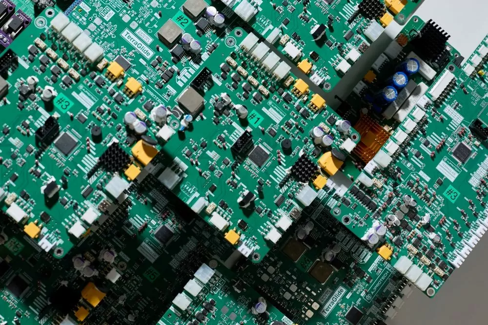
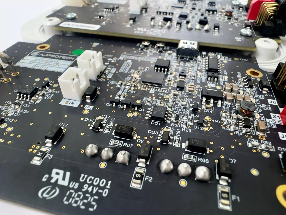
Component placement is the chess match of PCB design: every move shapes the outcome. The first rule of the game? Think like a manufacturer. Successful board design starts with the major actors like connectors, power supplies, and critical chips, anchored to best connect with outside devices or for easy access on the edge of your circuit board.
Next, the supporting cast comes in:
- High-speed components stay close to controllers
- Analog parts are kept far from digital clusters to prevent EMI
- Group related parts like decoupling capacitors, pull-ups, or series resistors near their peers
Always place components to streamline the layout process: this avoids a “spaghetti” signal mess and minimizes crossing traces. For high-speed circuits, the old rule applies: keep paths short and direct. Every added loop increases the risk of interference and signal loss.
Keep component orientation consistent to help assembly robots solder your PCB component army. Symmetrical placement makes automated inspection simpler, too, lowering the risk of hidden mistakes.
Always allow space for assembly tools: cramming parts too close causes issues during fabrication and later rework. The art of PCB layout lies in knowing when to step back. Plan for accessible test points for quality checks, your future self will thank you for it.

PCB Design Layout Guidelines for Best Performance
- Place sensitive analog circuits away from noisy digital areas
- Keep vias to a minimum, as each adds resistance and capacitance
- Set design rule checks early and stick to them: rules on trace width, clearance, and stack-up are essential
- Use modern PCB design software for real-time rule checking
- Lay out critical signals first, optimizing return paths
Never route signals beneath crystals or oscillators: these can suffer interference, putting your clock out of step. When in doubt, ask your printed circuit board manufacturer about preferred footprints and tolerances: early feedback beats a late-stage redesign every time.
At AJProTech, these practices are our foundation for reliable, manufacturable PCB design. To learn more about advanced concepts, see our hardware development guide.
Best Practices for PCB Design and Manufacturing
Establishing Effective PCB Design Rules
In PCB design, rules are more than polite suggestions: they’re guardrails that keep your circuit board safe and your timeline on track. The top commandment is aligning rules with your manufacturer’s capabilities.
For example, not every fabricator enjoys seeing microvias or razor-thin traces, so set trace width and spacing within what your manufacturer’s equipment can handle without sending warning emails.
- Request a design capabilities table from your PCB fab
- Set trace width, spacing, and via diameter rules based on current loads and equipment
- Never assume ultra-fine traces are possible
Rules do more than fit your board within fab specs, they also protect the board’s function. High-speed signal traces require tight impedance control, so set width and clearance tolerances based on your stack-up and materials. Require a solid ground plane, and assign keep-out areas for sensitive analog or high-speed signals.
Reference IPC-2221 or manufacturer-specific guidelines. Proper DRC (Design Rule Checking) in your PCB design software acts as your silent, ever-watchful friend, automating the hunt for violations. For reliable board layout, review, set, and rigorously enforce your rules from day one.
Guidelines for PCB Manufacturing and Assembly
To achieve manufacturability and cost-effectiveness, consider assembly during the design stage.
| Recommendation | Why It Matters | |
| Component placement | Place components for easy soldering, pick-and-place, and inspection | Simplifies assembly, reduces errors, improves inspection quality |
| Orientation & grouping | Group similar package types and orient polarized parts the same way | Speeds up assembly and minimizes placement mistakes |
| SMT side usage | Put surface-mount components on one side whenever possible | Reduces manufacturing complexity and cost |
| Clearances | Maintain clearances between leads, pads, and vias | Ensures proper solder flow and prevents shorts or defects |
| Thermal design | Use proper thermal reliefs and power planes under high-current components | Prevents overheating and local hotspots |
| Alignment features | Add fiducials and tooling holes | Enables accurate automated assembly and alignment |
| Panelization | Plan panelization for optimal yield and easy depanelization | Maximizes production efficiency and reduces waste |
| Edge spacing | Avoid placing components or ground pours too close to edges | Prevents damage during depanelization and handling |
For tips on optimizing your board for volume or prototyping, check hardware engineering best practices. Use a pre-release checklist: silkscreen clarity, polarity marks, part IDs, and solder mask expansion. These details seem small, but overlooking them can halt production.
